
 My Inquiry
 My Account


Infineon Technologies CY7C63923-PVXC
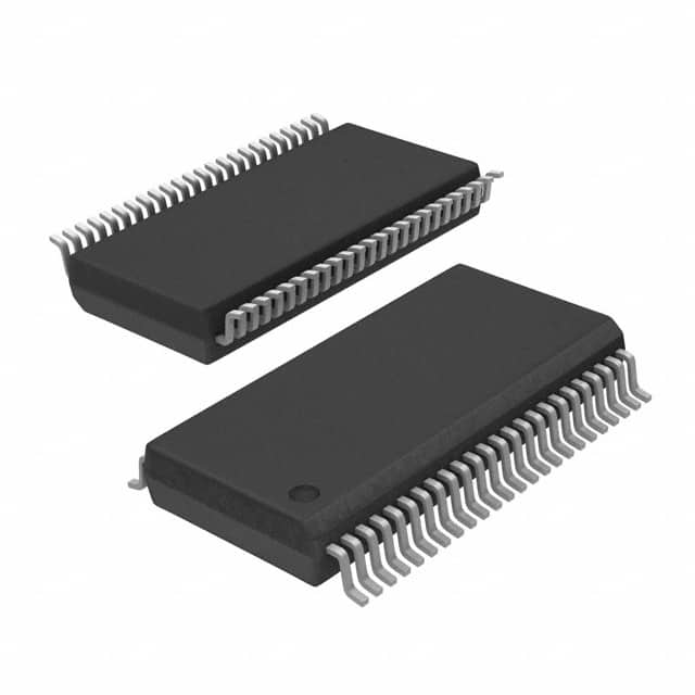
- Part No.:
- CY7C63923-PVXC
- Manufacturer:
- Infineon Technologies
- Category:
- Controllers
- Package:
- 48-BSSOP (0.295", 7.50mm Width)
- Datasheet:
-
 CY7C63923-PVXC.pdf
- Description:
- IC USB PERIPHERAL CTRLR 48SSOP
- Quantity:
- Payment:

- Shipping:

Inventory:4,373
Please send an inquiry. Send us your inquiry, and we will respond immediately.
Product details
Overview
CY7C63923-PVXC from Cypress Semiconductor is an enCoRe™ II 8-bit Flash-programmable microcontroller with integrated low-speed USB 2.0 and PS/2 interface, 48-pin SSOP package, 8 KB Flash, 256 bytes RAM, and internal 24 MHz oscillator ±1.5% accuracy. It serves as a peripheral controller in HID devices requiring dual-mode (USB/PS/2) operation without external crystals or pull-up resistors - e.g., optical mice and gaming controllers.
For engineers reviewing the CY7C63923-PVXC datasheet, CY7C63923-PVXC pinout, CY7C63923-PVXC application, or CY7C63923-PVXC equivalent, key selection criteria include its crystalless USB timing compliance, 36 GPIO with configurable 50-mA sink drive, dual-mode auto-configuration, integrated 3.3V regulator (125 mA), and capture timers for RF input edge timing in wireless peripherals.
Technical Context
The CY7C63923-PVXC implements a Harvard-architecture M8C CPU running up to 24 MHz, with USB Serial Interface Engine (SIE) supporting one device address, three endpoints (control + two data), and automatic D+/D– to PS/2 SCLK/SDATA reassignment. Its internal oscillator locks to USB traffic for ±1.5% timing accuracy without external crystal.
It integrates a 125-mA 3.3V regulator, programmable low-voltage detection, watchdog timer, and two 8-bit (or one 16-bit) capture timers tied to P0.5/TIO0 and P0.6/TIO1 - each storing independent rising/falling edge timestamps from the 16-bit free-running timer. GPIO ports 0–4 support maskable interrupts, open-drain outputs, and per-pin CMOS/TTL I/O configuration.
Key Specifications
| Parameter | Value and Actual Design Meaning |
|---|---|
| USB Speed | Low-Speed (1.5 Mbps); fully compliant with USB 2.0 and HID 1.1 specs - enables direct connection to host without external transceiver. |
| Memory | 8 KB Flash (with EEROM emulation) + 256 bytes RAM - sufficient for HID descriptor handling, firmware updates, and real-time event buffering. |
| GPIO Count | 36 pins across Ports 0–4; Port 0/1 individually configurable, Ports 2–4 group-configurable - supports complex peripheral interfacing with minimal external logic. |
| Timing Accuracy | ±1.5% internal oscillator tolerance under USB traffic - eliminates need for 12/24 MHz crystal while meeting LS-USB timing requirements. |
| Regulator Output | 125 mA @ 3.3V - powers external 3.3V sensors or LEDs directly, removing need for discrete LDO in space-constrained designs. |
| Capture Timers | Two 8-bit (or ganged 16-bit) edge-triggered timers on P0.5/P0.6 - captures precise rising/falling edge timestamps for RF remote decoding or encoder signal analysis. |
| Supply Range | 4.0 V to 5.25 V DC - compatible with standard USB bus-powered and wall-adapter systems without level-shifting. |
Pinout & Package
Package: 48-pin SSOP (0.300" wide), RoHS-compliant, surface-mount. Thermal pad not present; standard JEDEC MS-013AC footprint.
| Pin/Terminal | Circuit Role | Design Meaning |
|---|---|---|
| P0.0/CLKIN | GPIO Port 0 bit 0 / Clock Input | Configurable as oscillator input when external crystal enabled; otherwise functions as general-purpose I/O with interrupt capability. |
| P0.1/CLKOUT | GPIO Port 0 bit 1 / Clock Output | Drives external clock signal when crystal oscillator enabled; otherwise standard I/O with rising-edge interrupt (INT0). |
| P0.2/INT0 | GPIO Port 0 bit 2 / Interrupt 0 | Dedicated rising-edge interrupt source; no port-level grouping - enables fast response to critical events like button press. |
| P0.5/TIO0 | GPIO Port 0 bit 5 / Timer Input 0 | Primary input for 8-bit capture timer 0; stores timestamp of configured edge (rising/falling) from free-running timer. |
| P0.6/TIO1 | GPIO Port 0 bit 6 / Timer Input 1 | Primary input for 8-bit capture timer 1; independently latches edge timestamps - essential for dual-signal timing analysis (e.g., quadrature encoders). |
| P1.0/D+ | USB D+ / PS/2 SDATA | Bi-directional signal: USB differential data line or PS/2 serial data - auto-switched via firmware; includes internal 1.5-kΩ pull-up control. |
| P1.1/D– | USB D– / PS/2 SCLK | Bi-directional signal: USB differential data line or PS/2 clock - shares same auto-switching logic as P1.0; enables true dual-mode without GPIO mode pins. |
| P1.2/VREG | 3.3V Regulator Output | 125-mA regulated 3.3V supply output; powers external circuitry - eliminates need for discrete LDO in HID peripheral designs. |
| P1.3/SSEL | SPI Slave Select | Active-low SPI bus enable; TTL-threshold input - used to select this device as SPI slave during firmware updates or sensor communication. |
| P3.0–P3.7 | GPIO Port 3 (byte-configurable) | Group-configured 8-bit port; supports pull-up, open-drain, CMOS output - ideal for driving LED arrays or scanning keypad matrices. |
Key Features
| Feature | Design Value |
|---|---|
| Crystalless USB Timing | Internal oscillator dynamically tunes to USB traffic for ±1.5% accuracy - removes crystal, load capacitors, and board area in cost-sensitive HID designs. |
| Dual-Mode Auto-Switching | Single firmware handles both USB and PS/2 protocols using same D+/D– pins - no external switches, GPIO mode control, or PCB jumpers required. |
| High-Drive GPIO | Up to 50-mA sink current on designated pins (e.g., P1.5–P1.7) - directly drives LEDs, buzzers, or small relays without external drivers. |
| Edge-Capture Precision | Independent rising/falling edge timestamp storage per capture pin (P0.5/P0.6) - enables sub-microsecond timing resolution for RF remote decoding or motor commutation feedback. |
| In-System Reprogrammability | D+/D– pins double as programming interface - allows field firmware updates without dedicated debug header or programmer hardware. |
Applications
| Optical Mouse | Gaming Joystick |
|---|---|
|
Use Scenario: Optical sensor IC (e.g., ADNS-2610) streams motion data via SPI to controller; buttons and scroll wheel generate interrupts. IC Role / Device Role / Timing Role: USB peripheral controller with SPI master, GPIO interrupt handler, and low-speed USB SIE - manages HID report generation and transmission. Use Value: Internal 24 MHz oscillator ensures USB timing compliance without crystal; 50-mA GPIO sinks drive RGB status LEDs directly; capture timers decode quadrature signals from mechanical encoders. |
Use Scenario: Analog stick potentiometers and digital pushbuttons feed into ADC-less GPIO scanning; vibration motor and LED feedback require high-current drive. IC Role / Device Role / Timing Role: Dual-mode HID controller supporting both USB and PS/2 gamepad enumeration - auto-detects host interface at power-up. Use Value: No external components needed for mode switching; 125-mA 3.3V regulator powers analog sensor circuitry; programmable LVD prevents brown-out during battery operation. |
| Barcode Scanner | POS Terminal Keypad |
|
Use Scenario: Laser diode driver and photodiode amplifier interface via GPIO and analog comparator inputs; decoded data streamed as keyboard HID reports. IC Role / Device Role / Timing Role: Embedded peripheral controller with SPI master (for image sensor), capture timers (for pulse-width decoding), and USB HID endpoint management. Use Value: Edge-capture timers measure laser pulse widths with 1-µs resolution; internal pull-ups eliminate discrete resistors on scan trigger lines; 8 KB Flash accommodates multi-symbology decoding firmware. |
Use Scenario: Matrix keypad (4×4 or 5×6) scanned via Port 2/3; backlight LEDs driven by Port 1; USB cable connects to cash register or tablet. IC Role / Device Role / Timing Role: Low-power HID keyboard controller with wake-on-keypress, suspend-mode timer, and in-system firmware update capability. Use Value: 10-µA sleep current extends battery life in cordless POS units; 36 GPIO support large keypads without multiplexers; dual-mode support allows legacy PS/2 register compatibility. |
Equivalent & Alternatives
The following parts are listed as comparable options for similar low-speed USB peripheral controller applications.
| Alternative Part | Technical Difference | Application Difference | Selection Advice |
|---|---|---|---|
| CY7C63903-PC | 28-pin SSOP, 16 KB Flash, same core/peripherals but smaller I/O count (24 GPIO) and no Port 4 - lacks P4.0–P4.3 used for extended keypad or sensor expansion. | Targeted at simpler HID devices (e.g., basic keyboards) where 36 GPIO and 48-pin routing are unnecessary. | Select when BOM cost reduction and PCB area savings outweigh need for full GPIO scalability and capture timer flexibility. |
| CP2102N-A02-GM | USB-to-UART bridge (not MCU); no Flash, no GPIO, no PS/2 mode - requires external host processor for HID logic; only provides serial tunneling. | Suitable only for UART-based peripherals (e.g., thermal printers) where HID report generation occurs externally. | Choose only if application already uses external microcontroller and needs simple USB connectivity - not a functional replacement for CY7C63923-PVXC's embedded HID processing. |
Compared with CY7C63903-PC, the CY7C63923-PVXC offers 12 additional GPIO, Port 4 expansion, and identical capture timer functionality - critical for complex scanners or multi-function gamepads. Unlike CP2102N-A02-GM, it embeds full HID firmware execution, eliminating host dependency and enabling true standalone peripheral operation.
Availability
CY7C63923-PVXC is available at Aetrix Electronics and suitable for optical mouse development, gaming peripheral production, and industrial barcode scanner manufacturing requiring stable component supply across long-lifecycle programs.
Supply support for CY7C63923-PVXC includes scheduled delivery planning, volume procurement assistance, BOM continuity management, traceable sourcing, and lifecycle availability coordination for OEM customers, industrial embedded developers, connected-device designers, and electronics production programs.
Manufacturer
Cypress Semiconductor (now part of Infineon Technologies) is a fabless semiconductor company specializing in USB, memory, PSoC, and programmable system-on-chip solutions for embedded applications.
The enCoRe™ II product line was designed specifically for cost-sensitive, low-speed USB HID peripherals - integrating oscillator, regulator, pull-ups, and dual-mode logic to minimize bill-of-materials and PCB complexity.
FAQ
Does CY7C63923-PVXC support full-speed USB?
No. The CY7C63923-PVXC supports only Low-Speed USB (1.5 Mbps) per USB 2.0 specification. It lacks the transceiver circuitry and timing precision required for Full-Speed (12 Mbps) operation. Its internal oscillator and SIE are optimized exclusively for LS-USB timing compliance and HID-class enumeration.
Can the internal 3.3V regulator power external USB PHYs or level shifters?
No. The 125-mA 3.3V regulator is intended for low-power peripheral circuitry such as sensors, LEDs, or logic buffers - not for powering external USB PHYs, which typically require higher current stability and tighter regulation. External USB PHYs must use dedicated regulators meeting USB electrical specifications.
How is PS/2 mode activated without external hardware?
PS/2 mode is activated automatically when the host initiates PS/2 handshaking on D+/D– lines (P1.0/P1.1). Firmware detects the PS/2 start condition via internal logic and reconfigures the pins as SCLK/SDATA with 5-kΩ internal pull-ups - no GPIO pin assignment, external resistors, or mode-select strapping is required.
What is the maximum achievable resolution of the capture timers?
The capture timers resolve edge events with 1-µs granularity, derived from the 16-bit free-running timer clocked at 1 MHz (1 µs period). Each 8-bit capture register stores a programmable 8-bit window of that timer - enabling precise measurement of pulse widths or intervals up to 255 µs per capture, extendable to 65.5 ms when ganged as 16-bit.
CY7C63923-PVXC Specifications
- Product attributes
- Attribute value
- Manufacturer:
- Infineon Technologies
- Package/Case:
- 48-BSSOP (0.295", 7.50mm Width)
- Programmable:
- Not Verified
- Protocol:
- USB
- Function:
- Controller
- Interface:
- GPIO, SPI
- Standards:
- USB 2.0
- Voltage - Supply:
- 4V ~ 5.5V
- Current - Supply:
- 40mA
- Operating Temperature:
- 0°C ~ 70°C
- Supplier Device Package:
- 48-SSOP
- Grade:
- -
- Qualification:
- -
CY7C63923-PVXC FAQ
1.How can I place an order for CY7C63923-PVXC through Aetrix?
Please submit a Request for Quotation (RFQ) for CY7C63923-PVXC on Aetrix. Our sales agent will provide a competitive quotation and guide you through the order confirmation once you accept the terms.
2.Are the price and stock information for CY7C63923-PVXC reliable?
The price and inventory of CY7C63923-PVXC are updated periodically and may fluctuate due to market conditions. Stock and pricing data are typically refreshed every 24 hours. Quotation validity for CY7C63923-PVXC is usually 5 days.
3.What payment methods are accepted for CY7C63923-PVXC?
We accept Wire Transfer, PayPal, Credit Card, Western Union, MoneyGram, and Escrow for CY7C63923-PVXC transactions.
Note: Certain payment methods may incur a processing fee.
4.How is shipping managed for CY7C63923-PVXC?
CY7C63923-PVXC orders can be shipped via leading logistics carriers, including DHL, UPS, FedEx, TNT, or Registered Mail.
Once your CY7C63923-PVXC order is processed, you will receive an email with the shipment details and tracking number.
Note: Tracking information may take up to 24 hours to appear. Express delivery typically takes 3–5 business days.
5.How can I obtain technical support or documentation for CY7C63923-PVXC?
For technical support, including CY7C63923-PVXC datasheets, pinout diagrams, or application guidance, please contact our engineering support team. They can provide detailed documentation and assistance for your CY7C63923-PVXC requirements.
6.How does Aetrix verify that CY7C63923-PVXC is sourced from the original manufacturer or authorized distributors?
All CY7C63923-PVXC products on Aetrix are procured from qualified distributors and authorized channels. Our dedicated quality assurance team conducts strict verification, including traceability checks and, if necessary, third-party testing. This ensures that CY7C63923-PVXC meets industry standards.
7.What is the process for return or replacement of CY7C63923-PVXC?
All CY7C63923-PVXC units undergo pre-shipment inspection (PSI). If there is an issue with CY7C63923-PVXC, returns or replacements are accepted under the following conditions:
1.Quantity discrepancies, incorrect items, or visible external defects (such as breakage or corrosion), acknowledged by Aetrix.
2.The issue is reported within 90 days of delivery.
3.The CY7C63923-PVXC part is unused and in its original packaging.
Return procedure for CY7C63923-PVXC:
1.Submit a request within 90 days.
2.Obtain a Return Material Authorization (RMA) from Aetrix.
CY7C63923-PVXC Tags

-
PTN5150AHXMP
NXP USA Inc.

-
USB3740B-AI9-TR
Microchip Technology

-
USB3740B-AI2-TR
Microchip Technology

-
USB3300-EZK-TR
Microchip Technology
-
USB3300-EZK
Microchip Technology

-
FUSB340TMX
onsemi

-
FUSB302BMPX
onsemi

-
DP83826IRHBR
Texas Instruments

-
MCP2518FDT-E/QBB
Microchip Technology
-
FUSB302MPX
onsemi

-
MCP2518FDT-E/SL
Microchip Technology

-
FT260Q-R
FTDI, Future Technology Devices International Ltd
Tech Hub

An engineering guide to LED driver operation, constant-current and constant-voltage outputs, linear and switching topologies, dimming, IC selection, calculations, replacement compatibility, and fault c…

Operational amplifier guide covering op amp basics, feedback, ideal vs real op amps, common configurations, buffer circuits, offset, bias current, gain-bandwidth, slew rate, rail-to-rail limits and sel…

Jumper cables guide covering safe connection order, red and black clamp placement, final ground connection, cable gauge, length, clamp quality, copper vs CCA cables, jump starter comparison and battery…

LDO regulator guide covering low dropout voltage, power dissipation, thermal design, PSRR, output noise, capacitor stability, adjustable LDO circuits, LDO vs buck converter and datasheet selection chec…

Conditional Access Module guide covering CAM meaning, CI/CI+ interface, smart card authorization, DVB security workflow, TV and set-top box compatibility, internal electronics, ESD protection, connecto…

Guide to electronic component obsolescence covering EOL risk, PCN/PDN notices, last-time buy planning, replacement options, form-fit-function validation, counterfeit risk and BOM lifecycle management.

18650 battery guide covering lithium-ion cell basics, 3.6V/3.7V voltage, 4.2V charging, mAh and Wh capacity, protected cells, chargers, BMS, series-parallel packs, holders, welding and sourcing checks.…

Hall effect sensor guide covering working principle, linear and digital sensors, Arduino circuits, current sensing, speed detection, automotive applications, A3144 examples, signal filtering and datash…

Product Change Notification guide for electronic components, covering PCN meaning, PCN vs PDN/EOL, common change types, risk levels, form-fit-function review, engineering validation, BOM control, LTB/L…

A practical guide to blend door actuators, covering HVAC function, symptoms, location, AC and heater issues, reset and calibration, replacement cost, electrical diagnosis, compatibility checks, and rep…


