
 My Inquiry
 My Account


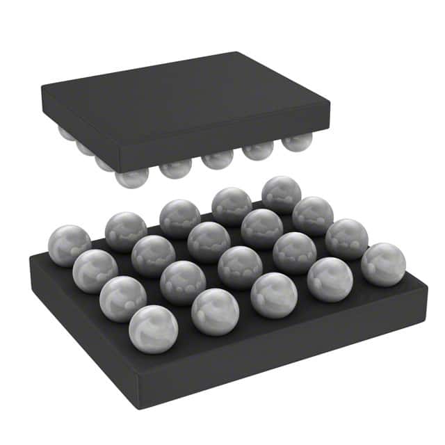
Cypress Semiconductor Corp CY7C68003-20FNXI
- Part No.:
- CY7C68003-20FNXI
- Manufacturer:
- Cypress Semiconductor Corp
- Category:
- Drivers, Receivers, Transceivers
- Package:
- 20-UFBGA, WLCSP
- Datasheet:
-
 CY7C68003-20FNXI.pdf
- Description:
- IC TRANSCEIVER FULL 1/1 20WLCSP
- Quantity:
- Payment:

- Shipping:

Inventory:1,240
Please send an inquiry. Send us your inquiry, and we will respond immediately.
Product details
Overview
CY7C68003-20FNXI from Cypress Semiconductor is a USB 2.0 Full Speed and High Speed compliant ULPI transceiver in a 20-pin WLCSP (2.14 × 1.76 mm, 0.4 mm pitch), supporting 1.8–3.3 V I/O, integrated 13/19.2/24/26 MHz PLL, and industrial temperature range (−40 °C to +85 °C). It operates in device mode only, integrates USB pull-up/termination resistors, and delivers 30 mA nominal active HS current with 5 µA sleep mode draw-optimized for mobile handset connectivity.
For engineers reviewing the CY7C68003-20FNXI datasheet, CY7C68003-20FNXI pinout, CY7C68003-20FNXI application, or CY7C68003-20FNXI equivalent, key selection criteria include ULPI SDR 8-bit interface compliance, multi-voltage I/O support, integrated oscillator/PLL architecture, UART pass-through capability via DP/DM, and WLCSP package constraints for space-constrained portable designs.
Technical Context
The CY7C68003-20FNXI implements UTMI+ Level 0 interface logic with full USB 2.0 FS/HS PHY compliance and supports synchronous ULPI data transfer at up to 60 MHz (SDR). Its internal PLL accepts 13, 19.2, 24, or 26 MHz reference inputs and generates precise USB clocking without external frequency synthesis.
It features dual power domains: 1.8 V core (VCC, 1.7–1.9 V), multi-range I/O (VIO, 1.7–3.6 V), and battery-supplied VBATT (3.0–5.775 V) feeding an internal 3.3 V regulator. The device supports five operation modes-including Normal, Sleep, ULPI Low Power, Carkit UART Pass-Through, and Configuration-with RESET_N-driven state transitions and no required power sequencing.
Key Specifications
| Parameter | Value and Actual Design Meaning |
|---|---|
| USB Compliance | Full Speed (12 Mbps) and High Speed (480 Mbps) per USB 2.0 specification; device-only mode. |
| ULPI Interface | 8-bit SDR data path, UTMI+ Level 0 compliant; supports 1.8–3.3 V I/O voltage auto-selection via VIO. |
| Reference Clock | 13 / 19.2 / 24 / 26 MHz crystal or LVCMOS input; fractional PLL ensures exact USB timing derivation. |
| Power Consumption | 5 µA nominal in Sleep Mode; 30 mA nominal during active HS transfer-enables battery-sensitive mobile use. |
| ESD Protection | JESD22-A114D 8 kV HBM (DP/DM/VSS); IEC61000-4-2 8 kV contact / 15 kV air discharge. |
| Operating Temperature | −40 °C to +85 °C industrial grade-validated for mobile handset thermal environments. |
| Package | 20-pin Wafer-Level Chip Scale Package (WLCSP), 2.14 × 1.76 mm, 0.4 mm pitch-designed for ultra-compact PCB layout. |
Pinout & Package
Package: 20-pin WLCSP (2.14 × 1.76 mm, 0.4 mm pitch), ball-grid layout with VSS and VSSBATT dedicated ground planes.
| Pin/Terminal | Circuit Role | Design Meaning |
|---|---|---|
| DP / DM | USB differential data pair | Direct connection to USB receptacle; integrated 1.5 kΩ pull-up resistor on DP for device enumeration. |
| VCC | Core supply | 1.8 V ±0.1 V (1.7–1.9 V) digital core power; must be stable before operation. |
| VIO | I/O supply | Configurable 1.8–3.3 V LVCMOS I/O domain; sets ULPI bus voltage level automatically. |
| VBATT | Battery input | 3.0–5.775 V input powering internal 3.3 V regulator for USBIO and XOSC blocks. |
| RESET_N | Active-low reset/control | Three-state control: assert ≥tSTATE to enter Sleep or Configuration Mode; must be pulled high if unused. |
| DATA[7:0] | ULPI bidirectional data bus | 8-bit SDR interface carrying commands, status, and packet data per ULPI v1.1 spec. |
| CLOCK / DIR / STP / NXT | ULPI control signals | Standard ULPI handshake lines; CLOCK is 60 MHz input from host controller, not generated by CY7C68003. |
| XI / XO | Oscillator interface | Crystal connections for 13/19.2/24/26 MHz parallel-resonant fundamental-mode crystal (12 pF load). |
Key Features
| Feature | Design Value |
|---|---|
| Integrated USB termination | On-die 1.5 kΩ DP pull-up and 15 kΩ DM termination resistors eliminate external components and reduce BOM count. |
| UART pass-through mode | Enables DP/DM pins to carry UART TXD/RXD signals (mapped to DATA[0]/DATA[1]) for hands-free car kit communication without additional PHY. |
| Multi-voltage I/O support | VIO pin auto-selects 1.8 V or 3.3 V signaling level-allows seamless interfacing with diverse host controllers across voltage domains. |
| Low-power sleep architecture | 5 µA quiescent current in Sleep Mode with full register retention-extends battery life in always-on portable devices. |
| Industrial-grade reliability | Qualified for −40 °C to +85 °C operation with 8 kV HBM ESD on DP/DM/VSS-meets mobile handset environmental requirements. |
Applications
| Mobile Handsets | Portable Media Players |
|---|---|
|
Use Scenario: Integration into smartphone baseband SoC subsystems requiring compact, low-power USB device connectivity. IC Role / Device Role / Timing Role: ULPI PHY layer bridging SoC UTMI+ interface to USB 2.0 receptacle; provides precise 480 Mbps HS clocking via internal PLL. Use Value: Eliminates discrete USB termination and oscillator components, reducing PCB area by >1.5 mm² and enabling sub-3 mm² total PHY footprint. |
Use Scenario: Enabling USB mass storage and firmware update in flash-based audio/video players with tight power budgets. IC Role / Device Role / Timing Role: USB 2.0 device transceiver handling enumeration, descriptor exchange, and bulk data transfers at up to 480 Mbps. Use Value: 5 µA sleep current extends playback time between charges; integrated 1.5 kΩ pull-up ensures reliable host detection without external bias. |
| DTV Set-Top Boxes | Portable GPS Receivers |
|
Use Scenario: Adding USB peripheral support (e.g., Wi-Fi dongles, storage) to embedded Linux-based DTV platforms. IC Role / Device Role / Timing Role: ULPI-compliant USB device PHY providing interoperability with standard Linux USB gadget drivers. Use Value: UTMI+ Level 0 compatibility ensures plug-and-play driver support; 30 mA active current avoids thermal throttling in enclosed enclosures. |
Use Scenario: Supporting USB-based firmware updates and NMEA data logging in battery-powered GPS navigation units. IC Role / Device Role / Timing Role: USB device endpoint managing CDC ACM class communication for GPS position streaming over USB virtual COM port. Use Value: UART pass-through mode allows reuse of DP/DM for legacy RS-232 GPS modules-reducing connector count and system cost. |
Equivalent & Alternatives
The following parts are listed as comparable options for similar USB 2.0 ULPI transceiver applications.
| Alternative Part | Technical Difference | Application Difference | Selection Advice |
|---|---|---|---|
| SMSC USB3317C-EZK | Supports both device and host modes; requires external 12 MHz crystal; no integrated UART pass-through. | Broader use in dual-role OTG systems; lacks Carkit UART mapping for automotive accessory integration. | Select when host capability or USB On-The-Go is required; avoid if strict device-only, low-pin-count, or car-kit UART reuse is needed. |
| Microchip USB2502-E/P | USB 2.0 hub controller (not transceiver); includes integrated hub logic, 2-port switching, and EEPROM configuration. | Used for multi-peripheral expansion-not suitable as direct ULPI PHY replacement. | Choose only for hub functionality; not a functional or pin-compatible alternative for CY7C68003-20FNXI's ULPI PHY role. |
Compared with SMSC USB3317C-EZK and Microchip USB2502-E/P, the CY7C68003-20FNXI offers unique value in ultra-compact device-only USB connectivity with integrated UART pass-through-making it optimal for space- and power-constrained mobile handsets where dual-role or hub functionality is unnecessary.
Availability
CY7C68003-20FNXI is available at Aetrix Electronics and suitable for mobile handsets, portable media players, DTV set-top boxes, and portable GPS receivers requiring stable component supply, long-term lifecycle support, and verified industrial temperature performance.
Supply support for CY7C68003-20FNXI includes scheduled delivery planning, volume procurement assistance, BOM continuity management, traceable sourcing, and lifecycle availability coordination for OEM customers, industrial embedded developers, connected-device designers, and electronics production programs.
Manufacturer
Cypress Semiconductor (now part of Infineon Technologies) is a fabless semiconductor company specializing in programmable system-on-chip (PSoC), memory, and USB connectivity solutions for embedded systems.
The MoBL-USB™ TX2UL product line was designed specifically for mobile handset and portable consumer electronics requiring minimal footprint, ultra-low power USB 2.0 device connectivity with integrated analog functions.
FAQ
Does CY7C68003-20FNXI support USB host mode?
No. The CY7C68003-20FNXI is a USB 2.0 device-only transceiver and does not implement host controller logic or UTMI+ host-side signaling. It connects exclusively as a peripheral to a USB host controller via ULPI interface and requires external host-side PHY or controller support.
What crystal specifications are required for XI/XO operation?
A parallel-resonant, fundamental-mode crystal with 13/19.2/24/26 MHz nominal frequency (±100 ppm tolerance), 750 µW drive level, 12 pF load capacitance (±5%), and ≤60 Ω ESR is required. Trace capacitance must be accounted for-typically 3 pF per side on FR4 PCBs.
How is UART pass-through mode enabled and used?
UART pass-through is activated by setting the Carkit Mode bit (bit 0) in the Interface Control Register during normal operation. DATA[0] maps to DM (TXD output), DATA[1] maps to DP (RXD input), and the internal USB clock is powered down-enabling DP/DM to function as a half-duplex UART link without external transceivers.
Is the 20-pin WLCSP package RoHS and REACH compliant?
Yes. The CY7C68003-20FNXI in 20-pin WLCSP packaging meets RoHS Directive 2011/65/EU and REACH Regulation (EC) No. 1907/2006 requirements, including lead-free solderability and absence of SVHC substances above threshold limits per manufacturer documentation.
CY7C68003-20FNXI Specifications
- Product attributes
- Attribute value
- Manufacturer:
- Cypress Semiconductor Corp
- Series:
- CY7C
- Package/Case:
- 20-UFBGA, WLCSP
- Packaging:
- Tray
- Product Status:
- Obsolete
- Type:
- Transceiver
- Protocol:
- USB 2.0
- Number of Drivers/Receivers:
- 1/1
- Duplex:
- Full
- Receiver Hysteresis:
- -
- Data Rate:
- -
- Voltage - Supply:
- 1.8V ~ 3.3V
- Operating Temperature:
- -40°C ~ 85°C
- Grade:
- -
- Qualification:
- -
- Mounting Type:
- Surface Mount
- Supplier Device Package:
- 20-WLCSP (2.14x1.76)
CY7C68003-20FNXI FAQ
1.How can I place an order for CY7C68003-20FNXI through Aetrix?
Please submit a Request for Quotation (RFQ) for CY7C68003-20FNXI on Aetrix. Our sales agent will provide a competitive quotation and guide you through the order confirmation once you accept the terms.
2.Are the price and stock information for CY7C68003-20FNXI reliable?
The price and inventory of CY7C68003-20FNXI are updated periodically and may fluctuate due to market conditions. Stock and pricing data are typically refreshed every 24 hours. Quotation validity for CY7C68003-20FNXI is usually 5 days.
3.What payment methods are accepted for CY7C68003-20FNXI?
We accept Wire Transfer, PayPal, Credit Card, Western Union, MoneyGram, and Escrow for CY7C68003-20FNXI transactions.
Note: Certain payment methods may incur a processing fee.
4.How is shipping managed for CY7C68003-20FNXI?
CY7C68003-20FNXI orders can be shipped via leading logistics carriers, including DHL, UPS, FedEx, TNT, or Registered Mail.
Once your CY7C68003-20FNXI order is processed, you will receive an email with the shipment details and tracking number.
Note: Tracking information may take up to 24 hours to appear. Express delivery typically takes 3–5 business days.
5.How can I obtain technical support or documentation for CY7C68003-20FNXI?
For technical support, including CY7C68003-20FNXI datasheets, pinout diagrams, or application guidance, please contact our engineering support team. They can provide detailed documentation and assistance for your CY7C68003-20FNXI requirements.
6.How does Aetrix verify that CY7C68003-20FNXI is sourced from the original manufacturer or authorized distributors?
All CY7C68003-20FNXI products on Aetrix are procured from qualified distributors and authorized channels. Our dedicated quality assurance team conducts strict verification, including traceability checks and, if necessary, third-party testing. This ensures that CY7C68003-20FNXI meets industry standards.
7.What is the process for return or replacement of CY7C68003-20FNXI?
All CY7C68003-20FNXI units undergo pre-shipment inspection (PSI). If there is an issue with CY7C68003-20FNXI, returns or replacements are accepted under the following conditions:
1.Quantity discrepancies, incorrect items, or visible external defects (such as breakage or corrosion), acknowledged by Aetrix.
2.The issue is reported within 90 days of delivery.
3.The CY7C68003-20FNXI part is unused and in its original packaging.
Return procedure for CY7C68003-20FNXI:
1.Submit a request within 90 days.
2.Obtain a Return Material Authorization (RMA) from Aetrix.
CY7C68003-20FNXI Tags

-
ATA6561-GAQW-N
Microchip Technology
-
ATA6561-GBQW-N
Microchip Technology

-
AM26LS32ACDR
Texas Instruments

-
SP485CN-L/TR
MaxLinear, Inc.
-
SP485EN-L/TR
MaxLinear, Inc.
-
SP485EEN-L/TR
MaxLinear, Inc.
-
SP485ECN-L/TR
MaxLinear, Inc.
-
THVD1400DR
Texas Instruments
-
AM26C31IDR
Texas Instruments

-
TLIN1021ADRQ1
Texas Instruments
-
MAX232IDR
Texas Instruments
-
AM26C32IDR
Texas Instruments
Tech Hub

An engineering guide to LED driver operation, constant-current and constant-voltage outputs, linear and switching topologies, dimming, IC selection, calculations, replacement compatibility, and fault c…

Operational amplifier guide covering op amp basics, feedback, ideal vs real op amps, common configurations, buffer circuits, offset, bias current, gain-bandwidth, slew rate, rail-to-rail limits and sel…

Jumper cables guide covering safe connection order, red and black clamp placement, final ground connection, cable gauge, length, clamp quality, copper vs CCA cables, jump starter comparison and battery…

LDO regulator guide covering low dropout voltage, power dissipation, thermal design, PSRR, output noise, capacitor stability, adjustable LDO circuits, LDO vs buck converter and datasheet selection chec…

Conditional Access Module guide covering CAM meaning, CI/CI+ interface, smart card authorization, DVB security workflow, TV and set-top box compatibility, internal electronics, ESD protection, connecto…

Guide to electronic component obsolescence covering EOL risk, PCN/PDN notices, last-time buy planning, replacement options, form-fit-function validation, counterfeit risk and BOM lifecycle management.

18650 battery guide covering lithium-ion cell basics, 3.6V/3.7V voltage, 4.2V charging, mAh and Wh capacity, protected cells, chargers, BMS, series-parallel packs, holders, welding and sourcing checks.…

Hall effect sensor guide covering working principle, linear and digital sensors, Arduino circuits, current sensing, speed detection, automotive applications, A3144 examples, signal filtering and datash…

Product Change Notification guide for electronic components, covering PCN meaning, PCN vs PDN/EOL, common change types, risk levels, form-fit-function review, engineering validation, BOM control, LTB/L…

A practical guide to blend door actuators, covering HVAC function, symptoms, location, AC and heater issues, reset and calibration, replacement cost, electrical diagnosis, compatibility checks, and rep…


