
 My Inquiry
 My Account


Infineon Technologies CY8C9540A-24PVXI
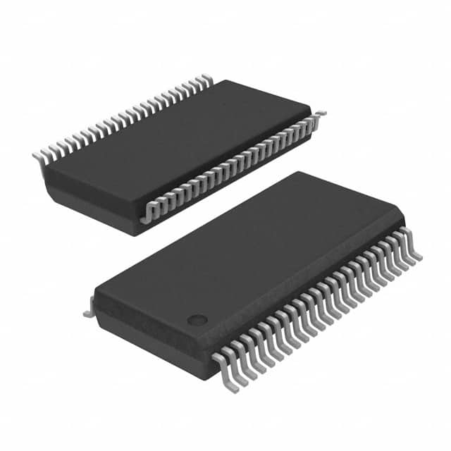
- Part No.:
- CY8C9540A-24PVXI
- Manufacturer:
- Infineon Technologies
- Category:
- I/O Expanders
- Package:
- 48-BSSOP (0.295", 7.50mm Width)
- Datasheet:
-
 CY8C9540A-24PVXI.pdf
- Description:
- IC XPNDR 100KHZ I2C 48SSOP
- Quantity:
- Payment:

- Shipping:

Inventory:307
Please send an inquiry. Send us your inquiry, and we will respond immediately.
Product details
Overview
CY8C9540A-24PVXI from Cypress Semiconductor is a 40-bit I/O expander IC with integrated EEPROM and eight independently configurable 8-bit PWM outputs, supporting I²C/SMBus-compatible communication with clock stretching, 3.3 V operation, and internal 11-Kbyte user-accessible EEPROM for persistent configuration storage. It serves as a dual-function I²C slave-simultaneously acting as a multi-port I/O controller and serial EEPROM-enabling GPIO expansion in space-constrained embedded control systems such as industrial HMIs and sensor interface modules.
For engineers reviewing the CY8C9540A-24PVXI datasheet, CY8C9540A-24PVXI pinout, CY8C9540A-24PVXI application, or CY8C9540A-24PVXI equivalent, key selection criteria include I²C address flexibility via Extendable Soft Addressing (A0–A6), interrupt-driven input change detection, EEPROM write-disable (WD) pin support, and per-pin drive mode configurability (strong drive, open-drain, pull-up/down, high-Z).
Technical Context
The device implements two independent I²C slave interfaces on a shared bus: one for register-mapped I/O control (using 7-bit base address 0x40/0x50 with A0–A6 extension), and another for EEPROM access (base address 0xA0/0xB0). All 40 I/O pins are grouped across GPort0–GPort5, with GPort1 and GPort2 offering configurable pins that double as address inputs (A1–A6) or write-disable (WD).
It features eight 8-bit PWM generators (PWM0–PWM7), each selectable per-pin via the Select PWM register and clocked by one of six internal sources (1.5 MHz, 93.75 kHz, 32 kHz, 24 MHz, or divided variants). Configuration registers-including Port Direction, Drive Mode, Inversion, and Interrupt Mask-are volatile but persistable to EEPROM using dedicated store/restore commands.
Key Specifications
| Parameter | Value and Actual Design Meaning |
|---|---|
| I/O Count | 40 bidirectional GPIO pins distributed across GPort0 (8-bit), GPort1 (5–8 bit), GPort2 (0–4 bit), GPort3 (8-bit), GPort4 (8-bit), GPort5 (4-bit) |
| PWM Outputs | 8 independent 8-bit PWM channels (PWM0–PWM7), each assignable to any I/O pin and configurable with period, pulse width, and clock source |
| EEPROM Size | 11-Kbyte user-accessible EEPROM with byte-level read/write, 2-byte addressing, and optional hardware write disable via WD pin |
| I²C Interface | Standard-mode (100 kHz) and fast-mode (400 kHz) compatible; requires master support for clock stretching; dual slave addressing (I/O expander + EEPROM) |
| Supply Voltage | 3.0 V to 3.6 V operation; internal power-on reset (POR) ensures deterministic startup state |
| Drive Modes | Per-pin selection among strong drive (10 mA source / 25 mA sink), open-drain, pull-up/pull-down, or high-impedance |
Pinout & Package
The CY8C9540A-24PVXI is housed in a 48-pin LQFP package (7 mm × 7 mm, 0.5 mm pitch) with exposed thermal pad. Pin functions are validated per Cypress Document 38-12036 Rev. *I (Page 6, "48-Pin Part Pinout").
| Pin/Terminal | Circuit Role | Design Meaning |
|---|---|---|
| Vdd | Power supply | 3.3 V core and I/O supply; decoupling required at pin |
| Vss | Ground | Digital ground reference for all I/O and internal logic |
| SCL | I²C clock input | Open-drain input requiring external pull-up; supports clock stretching |
| SDA | I²C data I/O | Open-drain bidirectional line; shares bus with SMBus devices |
| INT | Interrupt output | Active-low open-drain signal indicating input level or PWM state changes |
| WD | EEPROM write disable | Hardware lock: high = blocks all EEPROM writes; overrides register-based disable |
| A0–A6 | I²C address inputs | Extendable Soft Addressing: up to 128 unique addresses; unused pins repurposed as GPIO |
| GPort0–GPort5 | Configurable I/O banks | 40 total pins; each individually settable as input, output, quasi-bidirectional, or PWM output |
Key Features
| Feature | Design Value |
|---|---|
| Extendable Soft Addressing | Configurable I²C address using A0–A6 pins; unused address pins become functional GPIOs |
| User-Default EEPROM Storage | Port direction, drive mode, inversion, and PWM settings stored in dedicated EEPROM section and auto-restored at power-up |
| Interrupt-Driven Change Detection | INT pin asserts on input level transitions or PWM state changes; maskable per-pin via Interrupt Mask Register |
| Multi-Mode Per-Pin Drive Control | Seven drive modes per pin-including strong drive, open-drain, pull-up/down, and high-Z-configured via Drive Mode Registers (1Dh–23h) |
| Dual I²C Slave Functionality | Single physical device presents two logical slaves: I/O expander (0x40–0x7F) and EEPROM (0xA0–0xBF), accessed via MSb of command byte |
Applications
| Industrial HMI Panel Control | Smart Sensor Node Interface |
|---|---|
|
Use Scenario: Expanding microcontroller GPIO to drive LED indicators, pushbutton inputs, and relay controls on compact factory-floor HMIs. IC Role / Device Role / Timing Role: I/O expander with interrupt-driven input monitoring and PWM-controlled LED dimming; no external timing components required. Use Value: Reduces host MCU pin count burden while enabling local persistence of port states and brightness levels via on-chip EEPROM. |
Use Scenario: Aggregating analog sensor alerts, digital status flags, and calibration data storage in battery-powered environmental sensors. IC Role / Device Role / Timing Role: GPIO hub with nonvolatile error logging and configurable wake-up interrupts; EEPROM stores calibration offsets and fault history. Use Value: Eliminates need for discrete EEPROM and GPIO expanders, lowering BOM count and PCB area in space-constrained nodes. |
| Automotive Body Control Module | IoT Gateway Peripheral Management |
|
Use Scenario: Managing door lock actuators, interior lighting PWM, and switch inputs in low-voltage (3.3 V) body electronics submodules. IC Role / Device Role / Timing Role: Robust I²C I/O extender with watchdog timer and POR; WD pin enables hardware-locked EEPROM during firmware updates. Use Value: Ensures safe, fail-safe configuration retention across vehicle power cycles and ECU reprogramming events. |
Use Scenario: Centralizing control of Zigbee/Wi-Fi module status LEDs, SIM card detect lines, and USB port enable signals in edge gateways. IC Role / Device Role / Timing Role: Multi-function peripheral manager with interrupt aggregation and EEPROM-backed boot-time defaults. Use Value: Simplifies host SoC firmware by offloading GPIO state management and enabling field-updatable default configurations. |
Equivalent & Alternatives
The following parts are listed as comparable options for similar I/O expansion applications.
| Alternative Part | Technical Difference | Application Difference | Selection Advice |
|---|---|---|---|
| TCA6424A | 24-bit I/O expander with interrupt and reset; no integrated EEPROM or PWM; 1.65–5.5 V operation | Lacks nonvolatile configuration storage and PWM generation; suited for simpler GPIO extension without timing control | Select when only basic I²C GPIO expansion is needed and EEPROM/PWM are handled externally |
| PCA9555 | 16-bit I/O expander with interrupt; no EEPROM or PWM; supports higher I²C speeds (1 MHz Fast-mode Plus) | Lower I/O count and no on-chip memory; requires external EEPROM for persistent settings | Prefer for cost-sensitive, low-pin-count designs where host MCU handles configuration persistence |
Compared with TCA6424A and PCA9555, CY8C9540A-24PVXI uniquely integrates EEPROM-based configuration retention and eight PWM channels-reducing system-level component count and eliminating software overhead for state restoration and LED/timing control.
Availability
CY8C9540A-24PVXI is available at Aetrix Electronics and suitable for industrial HMI panels, smart sensor nodes, and automotive body control modules requiring stable component supply, long-term lifecycle support, and guaranteed traceable sourcing.
Supply support for CY8C9540A-24PVXI includes scheduled delivery planning, volume procurement assistance, BOM continuity management, traceable sourcing, and lifecycle availability coordination for OEM customers, industrial embedded developers, connected-device designers, and electronics production programs.
Manufacturer
Cypress Semiconductor (now part of Infineon Technologies) designs programmable system-on-chip solutions for embedded control, connectivity, and sensing applications, with global R&D and manufacturing infrastructure.
The CY8C95xxA family targets resource-constrained embedded systems needing scalable GPIO expansion, nonvolatile configuration, and integrated PWM-eliminating discrete logic and external memory in industrial and IoT edge devices.
FAQ
Does CY8C9540A-24PVXI support standard I²C masters without clock stretching?
No. The CY8C9540A-24PVXI requires I²C masters capable of clock stretching to accommodate internal EEPROM write cycles and register access latency. Masters that time out on stretched clocks-such as some SMBus controllers-will fail communication. Cypress confirms this requirement in Section 4 ("Device Access Addressing") and AC Electrical Characteristics (Page 19) of datasheet 38-12036 Rev. *I.
How is the 11-Kbyte EEPROM organized and accessed?
The EEPROM is byte-addressable using two-byte addressing (AHI/ALO), supporting up to 28 Kbytes; CY8C9540A uses 11 Kbytes. Reads and writes occur over the dedicated EEPROM I²C slave address (0xA0–0xBF). Writes are blocked if the WD pin is high or if the Config register disables EEPROM. User-default settings occupy a reserved EEPROM subsection and load automatically at power-on.
Can unused address pins (A1–A6) be used as general-purpose I/O?
Yes. When not assigned as I²C address bits in the Extendable Soft Addressing scheme, pins A1–A6 function as additional GPIOs within GPort1 or GPort2, as confirmed in Table 1 ("GPIO Availability") and Pin Descriptions (Page 9) of the datasheet. Their role is determined at runtime via configuration registers-not fixed at manufacture.
What happens to I/O states during power-up before EEPROM defaults are loaded?
At power-on, all I/O pins default to weak pull-up (factory setting) until the EEPROM-stored user defaults are loaded-typically within 10–20 ms after Vdd stabilization. This behavior is enforced by the internal Power-On Reset (POR) circuit and documented in the "Power-on-Reset" section (Page 1) and Register Descriptions (Page 12–13). No external initialization sequence is required.
CY8C9540A-24PVXI Specifications
- Product attributes
- Attribute value
- Manufacturer:
- Infineon Technologies
- Series:
- -
- Package/Case:
- 48-BSSOP (0.295", 7.50mm Width)
- Packaging:
- Tube
- Product Status:
- Active
- Programmable:
- Not Verified
- Number of I/O:
- 40
- Interface:
- I2C
- Interrupt Output:
- Yes
- Features:
- EEPROM, POR, PWM, WDT
- Output Type:
- Open Drain
- Current - Output Source/Sink:
- 10mA, 25mA
- Clock Frequency:
- 100 kHz
- Voltage - Supply:
- 3V ~ 5.25V
- Operating Temperature:
- -40°C ~ 85°C
- Grade:
- -
- Qualification:
- -
- Mounting Type:
- Surface Mount
- Supplier Device Package:
- 48-SSOP
CY8C9540A-24PVXI FAQ
1.How can I place an order for CY8C9540A-24PVXI through Aetrix?
Please submit a Request for Quotation (RFQ) for CY8C9540A-24PVXI on Aetrix. Our sales agent will provide a competitive quotation and guide you through the order confirmation once you accept the terms.
2.Are the price and stock information for CY8C9540A-24PVXI reliable?
The price and inventory of CY8C9540A-24PVXI are updated periodically and may fluctuate due to market conditions. Stock and pricing data are typically refreshed every 24 hours. Quotation validity for CY8C9540A-24PVXI is usually 5 days.
3.What payment methods are accepted for CY8C9540A-24PVXI?
We accept Wire Transfer, PayPal, Credit Card, Western Union, MoneyGram, and Escrow for CY8C9540A-24PVXI transactions.
Note: Certain payment methods may incur a processing fee.
4.How is shipping managed for CY8C9540A-24PVXI?
CY8C9540A-24PVXI orders can be shipped via leading logistics carriers, including DHL, UPS, FedEx, TNT, or Registered Mail.
Once your CY8C9540A-24PVXI order is processed, you will receive an email with the shipment details and tracking number.
Note: Tracking information may take up to 24 hours to appear. Express delivery typically takes 3–5 business days.
5.How can I obtain technical support or documentation for CY8C9540A-24PVXI?
For technical support, including CY8C9540A-24PVXI datasheets, pinout diagrams, or application guidance, please contact our engineering support team. They can provide detailed documentation and assistance for your CY8C9540A-24PVXI requirements.
6.How does Aetrix verify that CY8C9540A-24PVXI is sourced from the original manufacturer or authorized distributors?
All CY8C9540A-24PVXI products on Aetrix are procured from qualified distributors and authorized channels. Our dedicated quality assurance team conducts strict verification, including traceability checks and, if necessary, third-party testing. This ensures that CY8C9540A-24PVXI meets industry standards.
7.What is the process for return or replacement of CY8C9540A-24PVXI?
All CY8C9540A-24PVXI units undergo pre-shipment inspection (PSI). If there is an issue with CY8C9540A-24PVXI, returns or replacements are accepted under the following conditions:
1.Quantity discrepancies, incorrect items, or visible external defects (such as breakage or corrosion), acknowledged by Aetrix.
2.The issue is reported within 90 days of delivery.
3.The CY8C9540A-24PVXI part is unused and in its original packaging.
Return procedure for CY8C9540A-24PVXI:
1.Submit a request within 90 days.
2.Obtain a Return Material Authorization (RMA) from Aetrix.
CY8C9540A-24PVXI Tags
-
TCA6408ARSVR
Texas Instruments

-
TCA9535RTWR
Texas Instruments
-
FXL6408UMX
onsemi

-
PCF8574ADWR
Texas Instruments

-
PCF8574APWR
Texas Instruments
-
TCA9555PWR
Texas Instruments

-
TCA9554PWR
Texas Instruments
-
TCA9554APWR
Texas Instruments

-
TCA9539PWR
Texas Instruments
-
TCA9534PWR
Texas Instruments
-
TCA9555RTWR
Texas Instruments
-
TCA9535PWR
Texas Instruments
Tech Hub

Operational amplifier guide covering op amp basics, feedback, ideal vs real op amps, common configurations, buffer circuits, offset, bias current, gain-bandwidth, slew rate, rail-to-rail limits and sel…

Jumper cables guide covering safe connection order, red and black clamp placement, final ground connection, cable gauge, length, clamp quality, copper vs CCA cables, jump starter comparison and battery…

LDO regulator guide covering low dropout voltage, power dissipation, thermal design, PSRR, output noise, capacitor stability, adjustable LDO circuits, LDO vs buck converter and datasheet selection chec…

Conditional Access Module guide covering CAM meaning, CI/CI+ interface, smart card authorization, DVB security workflow, TV and set-top box compatibility, internal electronics, ESD protection, connecto…

Guide to electronic component obsolescence covering EOL risk, PCN/PDN notices, last-time buy planning, replacement options, form-fit-function validation, counterfeit risk and BOM lifecycle management.

18650 battery guide covering lithium-ion cell basics, 3.6V/3.7V voltage, 4.2V charging, mAh and Wh capacity, protected cells, chargers, BMS, series-parallel packs, holders, welding and sourcing checks.…

Hall effect sensor guide covering working principle, linear and digital sensors, Arduino circuits, current sensing, speed detection, automotive applications, A3144 examples, signal filtering and datash…

Product Change Notification guide for electronic components, covering PCN meaning, PCN vs PDN/EOL, common change types, risk levels, form-fit-function review, engineering validation, BOM control, LTB/L…

A practical guide to blend door actuators, covering HVAC function, symptoms, location, AC and heater issues, reset and calibration, replacement cost, electrical diagnosis, compatibility checks, and rep…

Engineering guide to Raspberry Pi alternatives, covering chip-level differences, Orange Pi, ROCK, Jetson, Banana Pi, NanoPi, Compute Module, Pico, GPIO, camera, HAT compatibility, and replacement risks…


