
 My Inquiry
 My Account


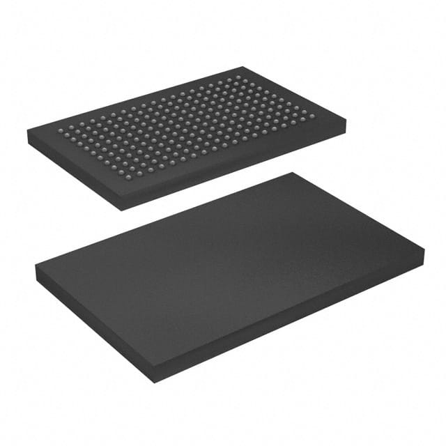
Infineon Technologies CYF0072V33L-133BGXI
- Part No.:
- CYF0072V33L-133BGXI
- Manufacturer:
- Infineon Technologies
- Category:
- FIFOs Memory
- Package:
- 209-BGA
- Datasheet:
-
 CYF0072V33L-133BGXI.pdf
- Description:
- IC FIFO SYNC 2MX36 10NS 209FBGA
- Quantity:
- Payment:

- Shipping:

Inventory:1,599
Please send an inquiry. Send us your inquiry, and we will respond immediately.
Product details
Overview
CYF0072V33L-133BGXI from Cypress Semiconductor is a 72-Mbit programmable first-in-first-out (FIFO) memory IC with independent 36-bit read/write ports, 133-MHz clock operation, LVCMOS 3.3 V I/O support, and configurable flag offsets for buffering high-speed data across asynchronous clock domains in networking and video systems.
For engineers reviewing the CYF0072V33L-133BGXI datasheet, CYF0072V33L-133BGXI pinout, CYF0072V33L-133BGXI application, or CYF0072V33L-133BGXI equivalent, key selection criteria include unidirectional ×36 bus width, JTAG boundary scan capability, programmable almost-empty/almost-full flags, and dual reset (MRS/PRS) for system-level synchronization and configuration retention.
Technical Context
The device implements a synchronous, unidirectional FIFO architecture with physically separate read and write address pointers, enabling simultaneous operations at up to 133 MHz with clock ratio tolerance of 0.5–2.0 between RCLK and WCLK. Memory organization is user-selectable via PORTSZ[2:0] pins across ×9 to ×36 word widths.
It integrates serial (SPI) and parallel programming interfaces for configuration registers, supports flow-through mailbox bypass, mark-and-retransmit functionality via MARK/RT pins, and provides DVal-synchronized output validity signaling. All control logic-including flag generation, pointer management, and reset sequencing-is implemented in dedicated on-die logic blocks surrounding the 72-Mbit SRAM array.
Key Specifications
| Parameter | Value and Actual Design Meaning |
|---|---|
| Memory density | 72 Mbit (8,388,608 × 9 bits, scalable to ×36) |
| Max clock frequency | 133 MHz - enables 4.8 Gbps peak throughput in ×36 mode |
| I/O voltage standard | LVCMOS 3.3 V - compatible with industrial 3.3 V logic families |
| Bus width support | ×9 / ×12 / ×16 / ×18 / ×20 / ×24 / ×32 / ×36 - selected by PORTSZ[2:0] |
| Operating temperature | –40 °C to +85 °C - qualified for industrial environment deployment |
| Reset modes | Master Reset (MRS) clears pointers, flags & config; Partial Reset (PRS) retains config registers |
| Status flags | EF, FF, HF, PAE, PAF - all synchronized to respective clocks (RCLK/WCLK) |
Pinout & Package
Package: 209-ball Fine-Pitch Ball Grid Array (FBGA), 13 mm × 13 mm, 0.8 mm pitch, RoHS-compliant.
| Pin/Terminal | Circuit Role | Design Meaning |
|---|---|---|
| WCLK, RCLK | Asynchronous clock inputs | Independent rising-edge-triggered clocks for write and read ports; ratio supported 0.5–2.0 |
| WEN, REN, IE, OE | Control enable signals | Enable/disable data transfer, input masking (IE), and output tri-state (OE) independently |
| D[35:0], Q[35:0] | Data I/O buses | 36-bit parallel interface; bus width dynamically configurable via PORTSZ[2:0] |
| MRS, PRS, MARK, RT | Function control inputs | Hardware-initiated master/partial reset, data marking, and retransmit triggering |
| FF, EF, HF, PAE, PAF, DVal | Status outputs | Active-low flags synchronized to WCLK (FF/HF/PAF) or RCLK (EF/PAE); DVal indicates valid Q[35:0] |
| SPI_SCLK, SPI_SI, SPI_SEN | Serial programming interface | 3-wire SPI port for loading flag offsets and configuration registers without halting FIFO operation |
| TCK, TMS, TDI, TDO | JTAG test interface | IEEE 1149.1-compliant boundary scan for PCB-level interconnect testing |
Key Features
| Feature | Design Value |
|---|---|
| Programmable flag offsets | Almost-empty/almost-full thresholds set via serial or parallel interface-enables precise buffer level control without firmware overhead |
| Flow-through mailbox register | Bypasses FIFO memory path to route data directly from D[35:0] to Q[35:0]-reduces latency for control messages or urgent payloads |
| Mark-and-retransmit | Hardware-accelerated data replay from user-marked location using MARK/RT pins-eliminates software pointer manipulation in streaming protocols |
| Dual reset architecture | MRS resets full state including configuration; PRS preserves programmed flag offsets and register settings-supports dynamic reinitialization in live systems |
| Multi-voltage I/O support | 3.3 V LVCMOS I/O with dedicated VCCIO supply-ensures signal integrity when interfacing with mixed-voltage SoCs or FPGAs |
Applications
| High-Speed Network Packet Buffering | Video Frame Synchronization |
|---|---|
|
Use Scenario: Buffering Ethernet frames between MAC and PHY layers operating at different clock domains (e.g., 125 MHz GMII vs. 156.25 MHz XAUI). IC Role / Device Role / Timing Role: Unidirectional FIFO with independent RCLK/WCLK domains absorbs timing skew and prevents packet loss during burst traffic. Use Value: 72-Mbit depth sustains >1.2 ms of 10-Gbps traffic; programmable PAF/PAE flags trigger DMA fetch before overflow, reducing CPU polling load. |
Use Scenario: Aligning frame capture (from image sensor) and display output (to HDMI controller) with mismatched pixel clocks. IC Role / Device Role / Timing Role: Clock-domain crossing buffer that decouples sensor readout (e.g., 74.25 MHz) from display refresh (e.g., 148.5 MHz). Use Value: ×36 bus width matches 36-bit parallel camera interfaces; HF flag triggers frame start detection, enabling real-time line-based processing. |
| Industrial Data Acquisition | Test Equipment Signal Streaming |
|
Use Scenario: Capturing high-resolution analog samples from multi-channel ADCs (e.g., 16-bit × 8 channels @ 100 MSPS) into FPGA memory. IC Role / Device Role / Timing Role: High-throughput write-side buffer absorbing ADC bursts while FPGA reads at lower sustained rate. Use Value: 133-MHz WCLK supports 4.8 Gbps write bandwidth; PRS allows on-the-fly buffer reset without losing calibration register settings. |
Use Scenario: Streaming waveform data from arbitrary function generator to digital pattern analyzer with jitter-tolerant handshake. IC Role / Device Role / Timing Role: Deterministic-latency FIFO ensuring bit-accurate delivery despite clock drift between instruments. Use Value: JTAG boundary scan validates PCB interconnect integrity pre-deployment; DVal synchronizes downstream logic to actual data availability-not clock edges. |
Equivalent & Alternatives
The following parts are listed as comparable options for similar programmable FIFO applications.
| Alternative Part | Technical Difference | Application Difference | Selection Advice |
|---|---|---|---|
| IDT72V2115L10PF | 36-Mbit depth, max 100 MHz, ×18/×36 only, no JTAG, 3.3 V only | Lacks mark/retransmit, mailbox, and serial programming; simpler flag set | Choose for cost-sensitive, fixed-configuration designs where 72-Mbit depth and advanced features are unnecessary |
| ON Semiconductor NB7L14M | Not a FIFO-dual 1:2 LVDS fanout buffer with integrated 2-bit delay; no memory | No buffering capability; serves clock distribution, not data domain bridging | Reject as non-equivalent-functionally incompatible for FIFO use cases requiring storage and pointer management |
Compared with IDT72V2115L10PF and NB7L14M, CYF0072V33L-133BGXI uniquely delivers 72-Mbit depth, hardware-assisted retransmit, and JTAG testability-making it the only viable option for high-reliability, multi-clock-domain systems requiring field-updatable flag thresholds and deterministic replay.
Availability
CYF0072V33L-133BGXI is available at Aetrix Electronics and suitable for high-speed network packet buffering, video frame synchronization, and industrial data acquisition requiring stable component supply across extended product lifecycles.
Supply support for CYF0072V33L-133BGXI includes scheduled delivery planning, volume procurement assistance, BOM continuity management, traceable sourcing, and lifecycle availability coordination for OEM customers, industrial embedded developers, connected-device designers, and electronics production programs.
Manufacturer
Cypress Semiconductor (now part of Infineon Technologies) designs high-performance memory and programmable logic solutions for industrial, automotive, and communications infrastructure markets.
CYF0072V33L-133BGXI belongs to the CYF00xxV family of programmable FIFOs engineered specifically for deterministic, low-latency data buffering across asynchronous clock domains in telecom, test equipment, and imaging systems.
FAQ
What is the maximum supported clock ratio between read and write clocks?
The CYF0072V33L-133BGXI supports a clock ratio range of 0.5 to 2.0 between RCLK and WCLK. This means the slower clock must be no less than half and no more than double the frequency of the faster clock. The device uses asynchronous pointer logic to maintain data integrity across this range without external handshaking.
How does the flow-through mailbox register operate?
When the MB pin is asserted, data presented on D[35:0] passes directly to Q[35:0] on the next RCLK edge, bypassing FIFO memory storage. This mode is used for urgent control words or status updates that require zero-latency delivery, independent of FIFO fill level or pointer state.
Can the almost-empty and almost-full flag offsets be changed during operation?
Yes-flag offsets are stored in configuration registers accessible via serial (SPI) or parallel programming modes. Offsets can be updated dynamically without resetting the FIFO or interrupting data flow, enabling adaptive buffer management based on real-time system load or error conditions.
Is JTAG boundary scan supported on this device?
Yes-the CYF0072V33L-133BGXI includes a fully compliant IEEE 1149.1 JTAG port (TCK/TMS/TDI/TDO) for boundary scan testing. It supports instruction register access, data register scanning, and IDCODE readback, enabling automated PCB interconnect verification during manufacturing.
CYF0072V33L-133BGXI Specifications
- Product attributes
- Attribute value
- Manufacturer:
- Infineon Technologies
- Series:
- -
- Package/Case:
- 209-BGA
- Packaging:
- Tray
- Product Status:
- Obsolete
- Programmable:
- Not Verified
- Memory Size:
- 72M (2M x 36)
- Function:
- Synchronous
- Data Rate:
- 133MHz
- Access Time:
- 10ns
- Voltage - Supply:
- 3 V ~ 3.6 V
- Current - Supply (Max):
- -
- Bus Directional:
- Uni-Directional
- Expansion Type:
- Width
- Programmable Flags Support:
- Yes
- Retransmit Capability:
- Yes
- FWFT Support:
- No
- Operating Temperature:
- -40°C ~ 85°C
- Mounting Type:
- Surface Mount
- Supplier Device Package:
- 209-FBGA (14x22)
CYF0072V33L-133BGXI FAQ
1.How can I place an order for CYF0072V33L-133BGXI through Aetrix?
Please submit a Request for Quotation (RFQ) for CYF0072V33L-133BGXI on Aetrix. Our sales agent will provide a competitive quotation and guide you through the order confirmation once you accept the terms.
2.Are the price and stock information for CYF0072V33L-133BGXI reliable?
The price and inventory of CYF0072V33L-133BGXI are updated periodically and may fluctuate due to market conditions. Stock and pricing data are typically refreshed every 24 hours. Quotation validity for CYF0072V33L-133BGXI is usually 5 days.
3.What payment methods are accepted for CYF0072V33L-133BGXI?
We accept Wire Transfer, PayPal, Credit Card, Western Union, MoneyGram, and Escrow for CYF0072V33L-133BGXI transactions.
Note: Certain payment methods may incur a processing fee.
4.How is shipping managed for CYF0072V33L-133BGXI?
CYF0072V33L-133BGXI orders can be shipped via leading logistics carriers, including DHL, UPS, FedEx, TNT, or Registered Mail.
Once your CYF0072V33L-133BGXI order is processed, you will receive an email with the shipment details and tracking number.
Note: Tracking information may take up to 24 hours to appear. Express delivery typically takes 3–5 business days.
5.How can I obtain technical support or documentation for CYF0072V33L-133BGXI?
For technical support, including CYF0072V33L-133BGXI datasheets, pinout diagrams, or application guidance, please contact our engineering support team. They can provide detailed documentation and assistance for your CYF0072V33L-133BGXI requirements.
6.How does Aetrix verify that CYF0072V33L-133BGXI is sourced from the original manufacturer or authorized distributors?
All CYF0072V33L-133BGXI products on Aetrix are procured from qualified distributors and authorized channels. Our dedicated quality assurance team conducts strict verification, including traceability checks and, if necessary, third-party testing. This ensures that CYF0072V33L-133BGXI meets industry standards.
7.What is the process for return or replacement of CYF0072V33L-133BGXI?
All CYF0072V33L-133BGXI units undergo pre-shipment inspection (PSI). If there is an issue with CYF0072V33L-133BGXI, returns or replacements are accepted under the following conditions:
1.Quantity discrepancies, incorrect items, or visible external defects (such as breakage or corrosion), acknowledged by Aetrix.
2.The issue is reported within 90 days of delivery.
3.The CYF0072V33L-133BGXI part is unused and in its original packaging.
Return procedure for CYF0072V33L-133BGXI:
1.Submit a request within 90 days.
2.Obtain a Return Material Authorization (RMA) from Aetrix.
CYF0072V33L-133BGXI Tags
-
7201LA15JGI
Renesas Electronics Corporation
-
7204L12JG
Renesas Electronics Corporation

-
72V82L15PAG8
Renesas Electronics Corporation

-
7205L15JGI
Renesas Electronics Corporation
-
7208L20JG
Renesas Electronics Corporation

-
72V2105L10PFG
Renesas Electronics Corporation
-
72V2111L15PFGI
Renesas Electronics Corporation

-
72V2113L6PFG
Renesas Electronics Corporation
-
72V36110L6PFG
Renesas Electronics Corporation

-
SN74ALVC7804-40DL
Texas Instruments
-
7202LA25JGI
Renesas Electronics Corporation
-
SN74V245-15PAG
Texas Instruments
Tech Hub

Operational amplifier guide covering op amp basics, feedback, ideal vs real op amps, common configurations, buffer circuits, offset, bias current, gain-bandwidth, slew rate, rail-to-rail limits and sel…

Jumper cables guide covering safe connection order, red and black clamp placement, final ground connection, cable gauge, length, clamp quality, copper vs CCA cables, jump starter comparison and battery…

LDO regulator guide covering low dropout voltage, power dissipation, thermal design, PSRR, output noise, capacitor stability, adjustable LDO circuits, LDO vs buck converter and datasheet selection chec…

Conditional Access Module guide covering CAM meaning, CI/CI+ interface, smart card authorization, DVB security workflow, TV and set-top box compatibility, internal electronics, ESD protection, connecto…

Guide to electronic component obsolescence covering EOL risk, PCN/PDN notices, last-time buy planning, replacement options, form-fit-function validation, counterfeit risk and BOM lifecycle management.

18650 battery guide covering lithium-ion cell basics, 3.6V/3.7V voltage, 4.2V charging, mAh and Wh capacity, protected cells, chargers, BMS, series-parallel packs, holders, welding and sourcing checks.…

Hall effect sensor guide covering working principle, linear and digital sensors, Arduino circuits, current sensing, speed detection, automotive applications, A3144 examples, signal filtering and datash…

Product Change Notification guide for electronic components, covering PCN meaning, PCN vs PDN/EOL, common change types, risk levels, form-fit-function review, engineering validation, BOM control, LTB/L…

A practical guide to blend door actuators, covering HVAC function, symptoms, location, AC and heater issues, reset and calibration, replacement cost, electrical diagnosis, compatibility checks, and rep…

Engineering guide to Raspberry Pi alternatives, covering chip-level differences, Orange Pi, ROCK, Jetson, Banana Pi, NanoPi, Compute Module, Pico, GPIO, camera, HAT compatibility, and replacement risks…


