
 My Inquiry
 My Account


onsemi CYII5SM1300AB-QWC
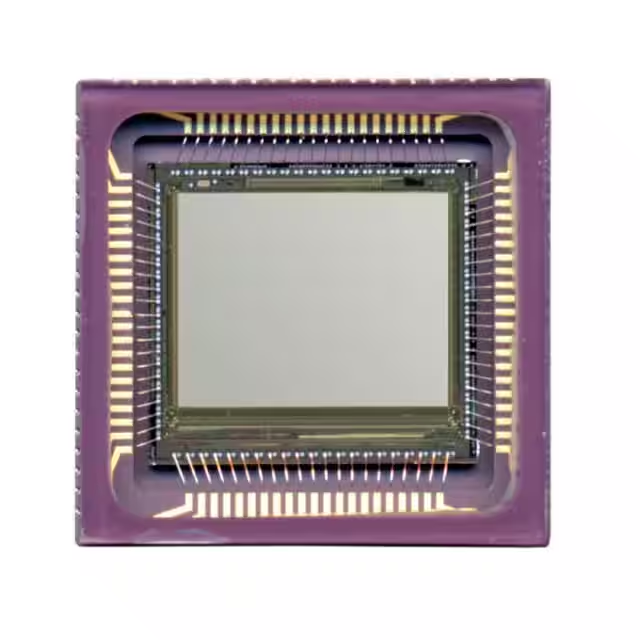
- Part No.:
- CYII5SM1300AB-QWC
- Manufacturer:
- onsemi
- Category:
- Image Sensors, Camera
- Package:
- 84-LCC
- Datasheet:
-
 CYII5SM1300AB-QWC.pdf
- Description:
- SENSOR IMAGE MONO CMOS 84-LCC
- Quantity:
- Payment:

- Shipping:

Inventory:4,993
Please send an inquiry. Send us your inquiry, and we will respond immediately.
Product details
Overview
CYII5SM1300AB-QWC from Cypress Semiconductor is a monochrome 1.3 MP CMOS image sensor with global and rolling shutter, 1280 × 1024 active pixels, 6.7 µm square pixels, and on-chip 10-bit ADC-designed for industrial machine vision systems requiring high-speed, low-noise imaging under controlled lighting.
For engineers reviewing the CYII5SM1300AB-QWC datasheet, pinout, applications, or equivalent options, key selection criteria include shutter mode flexibility (global/rolling), 27 fps full-frame performance, 84-pin LCC package compatibility, and analog output interface timing alignment with external ADCs.
Technical Context
The CYII5SM1300AB-QWC implements a 4-transistor pixel architecture enabling true global shutter operation via synchronized reset and sample control, while supporting rolling shutter for higher frame rates in sub-sampled modes. Its dual-Y-addressing register architecture separates readout and reset paths to eliminate smear during global exposure.
It integrates column-level fixed-pattern noise correction via double sampling, programmable gain/offset amplification (4-bit gain, 7-bit offset), and supports windowing down to 2×1 pixels. The analog output (PXL_OUT) operates at 40 MHz pixel rate with 260 Ω output impedance and requires external connection to ADC_IN (pin 69) for digitization.
Key Specifications
| Parameter | Value and Actual Design Meaning |
|---|---|
| Resolution | 1280 × 1024 active pixels - delivers 1.3 megapixel imaging with 2/3" optical format compatibility. |
| Pixel size | 6.7 µm × 6.7 µm - enables high fill factor and sensitivity of 8.4 V/lux·s at 650 nm. |
| Shutter types | Global and rolling shutter - supports motion-free capture (global) and high-speed ROI readout (rolling). |
| Frame rate | 27 fps at full resolution; up to 106 fps at 640 × 480 - enabled by programmable windowing and sub-sampling. |
| ADC resolution | 10-bit on-chip ADC - requires external routing from PXL_OUT (pin 28) to ADC_IN (pin 69); nominal 40 Msamples/s. |
| Power dissipation | 200 mW typical - distributed across analog (VDDA/VDDH/VDDR_LEFT), digital (VDDD), and pixel core (VDDC) supplies. |
| Operating temperature | 0 °C to +65 °C - specified for commercial industrial vision environments without extended thermal derating. |
| Supply voltages | Analog: 3.0–4.5 V; Digital/I/O: 3.3 V - requires separate stable rails; no internal power rejection circuitry. |
Pinout & Package
Package: 84-pin ceramic leadless chip carrier (LCC), hermetically sealed, glass-lid optional (QWC = no glass lid). Pin layout follows standard IBIS5-B-1300 floor plan with dedicated analog/digital/power/ground groups and signal isolation.
| Pin/Terminal | Circuit Role | Design Meaning |
|---|---|---|
| PXL_OUT (Pin 28) | Analog pixel output | Single-ended 40 MHz analog video stream; must be routed directly to external ADC_IN with minimal trace length and no vias. |
| ADC_IN (Pin 69) | ADC input | External connection point for PXL_OUT; not internally connected-requires PCB-level wiring. |
| VDDA (Pins 1, 3, 5, 7, 9) | Analog supply | +3.0–3.6 V for image core analog circuitry; highly sensitive to noise-requires local decoupling. |
| VDDD (Pins 2, 4, 6, 8, 10) | Digital supply | +3.0–3.6 V for sequencer, registers, and digital logic; separate ground (GNDD) required. |
| VDDH (Pin 12) | HOLD switch voltage | +3.3–4.5 V for sample/hold switches; critical for global shutter timing integrity. |
| VDDR_LEFT (Pin 13) | Pixel reset voltage | +3.3–4.5 V; highest reset rail-determines full-well capacity (62500 e⁻) and dynamic range. |
| SYS_CLOCK (Pin 15) | Master clock input | 40 MHz max; drives all internal timing including pixel rate, sequencer, and ADC synchronization. |
| Y_START / Y_CLOCK (Pins 17–18) | Vertical addressing control | Initiates row readout sequence; timing-critical for frame sync and blanking intervals. |
| SPI_CS / SPI_SCLK / SPI_MOSI (Pins 20–22) | Serial configuration interface | 3-wire SPI for register programming (shutter mode, gain, offset, windowing, sub-sampling). |
| GNDA / GNDD / GND_AB (Pins 24, 26, 27) | Analog/digital/anti-blooming grounds | Must be isolated on PCB; GND_AB prevents charge overflow in bright scenes. |
Key Features
| Feature | Design Value |
|---|---|
| Programmable region-of-interest (ROI) | Enables arbitrary X/Y start/stop coordinates-supports digital zoom down to 2×1 pixel window for inspection targeting. |
| Double-slope integration | Extends dynamic range beyond 64 dB in rolling shutter mode by capturing two exposures per pixel line. |
| On-chip FPN correction | Double sampling eliminates fixed pattern noise from both pixel array and column amplifiers-reducing FPN to 4.5 LSB10. |
| Sub-sampling modes | Configurable 1:2 reduction (X/Y) with SWAP_12/SWAP_30 controls-maintains field of view while doubling frame rate. |
| Gain/offset calibration | 4-bit programmable amplifier gain (1.37×–12.42×) and 7-bit DAC-controlled offset-enables precise signal mapping to ADC input range (1–3 V). |
| Multi-slope global shutter | Up to 4 slopes per integration cycle-captures high-dynamic-range scenes (e.g., reflective metal + shadowed features) without motion blur. |
Applications
| Machine Vision Inspection | Traffic Monitoring |
|---|---|
Use Scenario: High-precision dimensional measurement of PCB solder joints under strobed LED illumination. IC Role / Device Role / Timing Role: CYII5SM1300AB-QWC acts as the primary image acquisition engine with global shutter to freeze motion of conveyor-belt-mounted boards. Use Value: 6.7 µm pixels resolve <100 µm features; 27 fps enables real-time pass/fail decision at 0.5 m/s belt speed. | Use Scenario: License plate recognition at intersections under variable ambient light and vehicle motion. IC Role / Device Role / Timing Role: CYII5SM1300AB-QWC captures synchronized frames using rolling shutter ROI readout centered on lane markers. Use Value: 106 fps at 640 × 480 ensures ≥3 usable frames per passing vehicle; monochrome response maximizes contrast in grayscale IR illumination. |
| Industrial Robotics Guidance | Automated Optical Sorting |
Use Scenario: Bin-picking robot identifying randomly oriented metal parts on vibrating feeder trays. IC Role / Device Role / Timing Role: CYII5SM1300AB-QWC provides low-latency image stream with programmable windowing to track part centroids. Use Value: Sub-sampling maintains 50+ fps at reduced resolution while preserving field-of-view-critical for closed-loop servo response. | Use Scenario: Food processing line rejecting defective produce based on surface blemish detection. IC Role / Device Role / Timing Role: CYII5SM1300AB-QWC acquires uniform-lit monochrome images optimized for edge-based defect segmentation. Use Value: 64 dB SNR and 2.5 LSB10 temporal noise ensure reliable thresholding of sub-pixel defects under 5000 K white LED lighting. |
Equivalent & Alternatives
The following parts are listed as comparable options for similar CMOS image sensor applications.
| Alternative Part | Technical Difference | Application Difference | Selection Advice |
|---|---|---|---|
| ON Semiconductor AR0130CS | 1.2 MP, 12-bit ADC, 1/3" optical format, rolling shutter only; lower sensitivity (4.2 V/lux·s). | Lacks global shutter-unsuitable for moving-target metrology; better power efficiency (120 mW). | Select when cost-sensitive, static-scene applications dominate and global shutter is unnecessary. |
| ams AS5700-40 | 1.3 MP, 10-bit ADC, 2/3" format, global + rolling shutter; higher dark current (12 e⁻/sec) and narrower temp range (−20 °C to +60 °C). | Supports extended temperature but exhibits higher thermal noise-requires active cooling for long-exposure inspection. | Select when operating below 0 °C is required, accepting trade-off in dark noise performance. |
Compared with AR0130CS and AS5700-40, the CYII5SM1300AB-QWC uniquely balances global/rolling shutter duality, 6.7 µm pixel sensitivity, and 0–65 °C operation-making it optimal for factory-floor machine vision where motion artifact elimination and ambient thermal stability are co-critical.
Availability
CYII5SM1300AB-QWC is available at Aetrix Electronics and suitable for machine vision inspection, traffic monitoring, industrial robotics guidance, and automated optical sorting requiring stable component supply across multi-year production cycles.
Supply support for CYII5SM1300AB-QWC includes scheduled delivery planning, volume procurement assistance, BOM continuity management, traceable sourcing, and lifecycle availability coordination for OEM customers, industrial embedded developers, connected-device designers, and electronics production programs.
Manufacturer
Cypress Semiconductor (now part of Infineon Technologies) designs high-performance mixed-signal ICs for industrial, automotive, and IoT applications, with emphasis on reliability and system-level integration.
The IBIS5 family-including CYII5SM1300AB-QWC-is engineered specifically for demanding industrial vision systems requiring deterministic shutter control, low-noise analog signal chains, and robust packaging for factory environments.
FAQ
What shutter modes does the CYII5SM1300AB-QWC support, and how do they differ in use?
The CYII5SM1300AB-QWC supports both global and rolling shutter. Global shutter captures all pixels simultaneously-essential for motion-free imaging of fast-moving objects like conveyor belts. Rolling shutter reads rows sequentially, enabling higher frame rates (up to 106 fps at reduced resolution) but introducing skew in moving scenes. Selection is configured via sequencer registers and affects bias voltage settings (e.g., VDDH/VDDR_LEFT at +4.5 V for global mode).
How is the analog output of the CYII5SM1300AB-QWC interfaced to an external ADC?
The CYII5SM1300AB-QWC outputs analog pixel data on PXL_OUT (pin 28), which must be externally wired to ADC_IN (pin 69). This connection is not internal-the sensor lacks an integrated ADC path. Routing must use short, direct top-layer traces (<10 mm), avoid vias, and maintain 260 Ω impedance matching to preserve 40 MHz signal fidelity and minimize noise coupling.
Does the CYII5SM1300AB-QWC include on-chip fixed pattern noise (FPN) correction, and how is it implemented?
Yes, the CYII5SM1300AB-QWC implements on-chip FPN correction via double sampling: each pixel's signal and reset level are sampled separately in column amplifiers, then subtracted to cancel pixel-to-pixel and amplifier offset variations. This reduces measured FPN to 4.5 LSB10 and is active in both global and rolling shutter modes without user intervention.
What are the power supply requirements for the CYII5SM1300AB-QWC, and why are separate analog/digital rails critical?
The CYII5SM1300AB-QWC requires three independent supply groups: analog (VDDA/VDDH/VDDR_LEFT, 3.0–4.5 V), digital (VDDD, 3.0–3.6 V), and I/O (3.3 V). Separate rails are critical because the sensor has no on-chip power rejection-any noise on VDDA directly modulates pixel output, increasing temporal noise. Local 100 nF + 10 µF decoupling at each supply pin is mandatory.
Can the CYII5SM1300AB-QWC perform region-of-interest (ROI) readout, and what is the minimum window size?
Yes, the CYII5SM1300AB-QWC supports fully programmable ROI readout via user-defined row/column start/stop addresses. The minimum configurable window is 2×1 pixels-achieved by setting X_START=X_END=0 and Y_START=Y_END=0 in the sequencer registers. This enables extreme digital zoom for high-magnification inspection without resampling artifacts.
CYII5SM1300AB-QWC Specifications
- Product attributes
- Attribute value
- Manufacturer:
- onsemi
- Series:
- -
- Package/Case:
- 84-LCC
- Packaging:
- Tray
- Product Status:
- Obsolete
- Type:
- CMOS
- Pixel Size:
- 6.7µm x 6.7µm
- Active Pixel Array:
- 1280H x 1024V
- Frames per Second:
- 27.0
- Voltage - Supply:
- 3V ~ 4.5V
- Supplier Device Package:
- 84-LCC (18x18)
- Operating Temperature:
- -
- Grade:
- -
- Qualification:
- -
CYII5SM1300AB-QWC FAQ
1.How can I place an order for CYII5SM1300AB-QWC through Aetrix?
Please submit a Request for Quotation (RFQ) for CYII5SM1300AB-QWC on Aetrix. Our sales agent will provide a competitive quotation and guide you through the order confirmation once you accept the terms.
2.Are the price and stock information for CYII5SM1300AB-QWC reliable?
The price and inventory of CYII5SM1300AB-QWC are updated periodically and may fluctuate due to market conditions. Stock and pricing data are typically refreshed every 24 hours. Quotation validity for CYII5SM1300AB-QWC is usually 5 days.
3.What payment methods are accepted for CYII5SM1300AB-QWC?
We accept Wire Transfer, PayPal, Credit Card, Western Union, MoneyGram, and Escrow for CYII5SM1300AB-QWC transactions.
Note: Certain payment methods may incur a processing fee.
4.How is shipping managed for CYII5SM1300AB-QWC?
CYII5SM1300AB-QWC orders can be shipped via leading logistics carriers, including DHL, UPS, FedEx, TNT, or Registered Mail.
Once your CYII5SM1300AB-QWC order is processed, you will receive an email with the shipment details and tracking number.
Note: Tracking information may take up to 24 hours to appear. Express delivery typically takes 3–5 business days.
5.How can I obtain technical support or documentation for CYII5SM1300AB-QWC?
For technical support, including CYII5SM1300AB-QWC datasheets, pinout diagrams, or application guidance, please contact our engineering support team. They can provide detailed documentation and assistance for your CYII5SM1300AB-QWC requirements.
6.How does Aetrix verify that CYII5SM1300AB-QWC is sourced from the original manufacturer or authorized distributors?
All CYII5SM1300AB-QWC products on Aetrix are procured from qualified distributors and authorized channels. Our dedicated quality assurance team conducts strict verification, including traceability checks and, if necessary, third-party testing. This ensures that CYII5SM1300AB-QWC meets industry standards.
7.What is the process for return or replacement of CYII5SM1300AB-QWC?
All CYII5SM1300AB-QWC units undergo pre-shipment inspection (PSI). If there is an issue with CYII5SM1300AB-QWC, returns or replacements are accepted under the following conditions:
1.Quantity discrepancies, incorrect items, or visible external defects (such as breakage or corrosion), acknowledged by Aetrix.
2.The issue is reported within 90 days of delivery.
3.The CYII5SM1300AB-QWC part is unused and in its original packaging.
Return procedure for CYII5SM1300AB-QWC:
1.Submit a request within 90 days.
2.Obtain a Return Material Authorization (RMA) from Aetrix.
CYII5SM1300AB-QWC Tags

-
MT9M114EBLSTCZ-CR
onsemi
-
EPC611-CSP24-001
ESPROS Photonics AG
-
AR0147ATSC00XUEG5-DRBR
onsemi
-
AR0130CSSM00SPCA0-DRBR
onsemi
-
AR1335CSSC11SMKA0-CP
onsemi
-
AR0521SR2M09SURA0-DP
onsemi
-
AR0135CS2M25SUEA0-DPBR
onsemi
-
AR0522SRSC09SURA0-DP
onsemi
-
AR0134CSSC00SPCA0-DPBR
onsemi
-
AR0134CSSM00SUEA0-DPBR
onsemi
-
AR0521SR2C09SURA0-DP
onsemi
-
AR0135CS2M00SUEA0-DPBR
onsemi
Tech Hub

Counterfeit components can hide behind convincing markings and passing basic function tests. This engineering reference covers source traceability, external inspection, X-ray, XRF, electrical testing, …

A practical engineering and sourcing framework covering lifecycle verification, lifetime-buy calculations, replacement qualification, supplier checks and counterfeit-risk controls.

TTL and CMOS logic families differ in thresholds, loading, output drive, power and timing. This engineering guide compares 74HC and 74HCT, calculates noise margins and checks 3.3 V/5 V compatibility.

A practical engineering guide to 3.3V and 5V logic compatibility, input thresholds, resistor dividers, translator ICs, MOSFET level shifting, I2C pull-ups, timing limits and power-sequencing risks.

The 74HC595 uses push-pull logic outputs, while the TPIC6B595 uses 50 V open-drain DMOS sinks for higher-power loads. This guide compares timing, current limits, 3.3 V interfacing, load wiring, thermal…

The 74HC595 converts serial data into eight stable parallel outputs. This guide covers pin functions, shift and storage timing, OE and MR behavior, drive-current limits, cascading, voltage compatibilit…

A technical comparison of level-sensitive latches and edge-triggered flip-flops, covering timing windows, setup and hold limits, master–slave operation, time borrowing, race-through, HDL inference and…

A D latch stores one bit while Enable controls when data can pass. This reference covers gate-level operation, truth tables, transparency, setup and hold timing, LE versus OE, common ICs and practical …

An SR latch stores one bit through cross-coupled feedback. This engineering reference covers NOR and NAND implementations, truth tables, forbidden-state recovery, gated operation, switch debouncing, fa…

Latch circuits retain one bit through feedback. This technical reference covers SR and D latches, truth tables, transparency, timing limits, latch-versus-flip-flop behavior, applications and common log…


