
 My Inquiry
 My Account


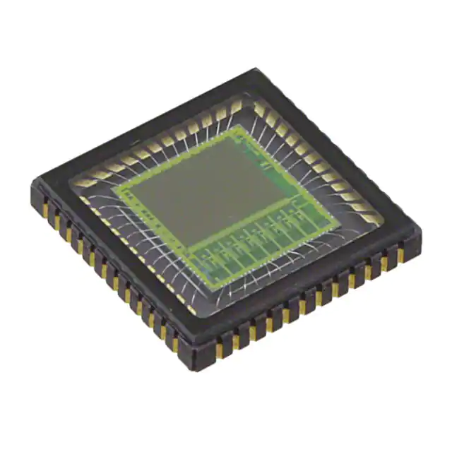
onsemi CYIL1SM0300AA-QDC
- Part No.:
- CYIL1SM0300AA-QDC
- Manufacturer:
- onsemi
- Category:
- Image Sensors, Camera
- Package:
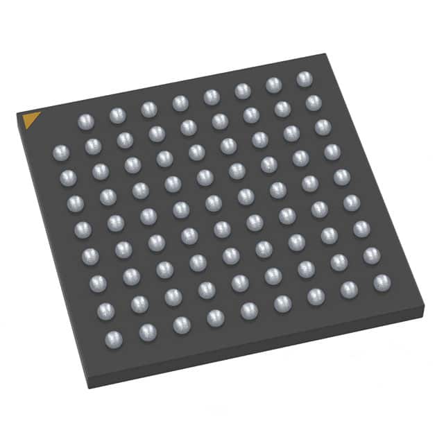
- 48-LCC
- Datasheet:
-
 CYIL1SM0300AA-QDC.pdf
- Description:
- SENSOR IMAGE MONO CMOS 48-LCC
- Quantity:
- Payment:

- Shipping:

Inventory:4,157
Please send an inquiry. Send us your inquiry, and we will respond immediately.
Product details
Overview
CYIL1SM0300AA-QDC from Cypress Semiconductor is a monochrome VGA CMOS image sensor with global electronic snapshot shutter, 640 × 480 active pixels, 9.9 µm square pixel pitch, on-chip 10-bit ADCs, and 80 MHz pixel rate - deployed in machine vision systems requiring high-speed motion capture and precise frame synchronization.
For engineers reviewing the CYIL1SM0300AA-QDC datasheet, pinout, applications, or equivalent options, this page delivers verified electro-optical specs, SPI-configurable ROI/windowing, subsampling support, programmable gain/offset calibration, and LCC-48 package integration guidance for real-time imaging designs.
Technical Context
The CYIL1SM0300AA-QDC implements a pipelined snapshot shutter architecture with simultaneous pixel reset and integration, enabling true global exposure across all 640 × 480 pixels. Its 6-transistor (6T) pixel design achieves 3200 V·m²/W·s responsivity and 61 dB dynamic range while maintaining low parasitic light sensitivity (1/5000).
Readout uses four parallel 10-bit pipelined ADCs operating at 20 Msamples/s each, multiplexed to a single 80 MHz digital output bus. Programmable gain (×1–×16 in 16 steps) and offset (256-step DAC) are applied via SPI before ADC conversion, with input range mapped to 0.75–1.75 V to preserve FPN correction headroom.
Key Specifications
| Parameter | Value and Actual Design Meaning |
|---|---|
| Resolution | 640 × 480 active pixels - supports VGA-standard optical interface and lens compatibility. |
| Pixel size | 9.9 µm × 9.9 µm - yields 6.3 mm × 4.7 mm active area matching ½-inch optical format. |
| Shutter type | Electronic pipelined snapshot shutter - enables synchronized global exposure with integration during readout. |
| Max frame rate | 250 fps at full resolution - scalable to 1076 fps via 256 × 256 windowing or 488 fps via Y-sub-sampling. |
| ADC resolution | On-chip 10-bit ADCs - four parallel converters deliver 80 MSPS aggregate throughput with DNL < 0.3 LSB. |
| Dynamic range | 61 dB typical - extendable to ~90 dB using dual/triple slope modes for high-contrast scenes. |
| Power supply | Analog: 2.5 V (VDDA/VPIX/VADC); Digital: 2.5 V (VDDD); I/O: 2.5 V - requires separate low-noise rails per domain. |
| Operating temp | –40°C to +70°C - validated for industrial machine vision environments with dark current degradation limits. |
Pinout & Package
Package: 48-pin ceramic leadless chip carrier (LCC), hermetically sealed with integrated cover glass (QDC variant). Dimensions: 12.7 mm × 12.7 mm × 2.54 mm (JEDEC MS-026AC).
| Pin/Terminal | Circuit Role | Design Meaning |
|---|---|---|
| CLK | Master pixel clock input | Accepts 80 MHz square/sine wave; drives internal sequencer and ADC sampling timing. |
| LINE_VALID | Digital output strobe | Active-high pulse indicates valid pixel data present on parallel output bus. |
| FRAME_VALID | Digital output strobe | Active-high pulse marks start of new frame; used for external frame synchronization. |
| RESET_N | Active-low sequencer reset | Asynchronous reset of internal timing generator; must be held low during register updates. |
| SPI_ENABLE | Serial interface enable | Activates SPI controller; required before SPI_CLK/SPI_DATA transactions. |
| SPI_CLK | SPI clock input | Up to 20 MHz; synchronous with register writes/reads during Frame Overhead Time (FOT). |
| SPI_DATA | Bidirectional serial data | Transfers 11-bit register addresses and 8–12-bit configuration values per SPI transaction. |
| VDDA / VDDD / VADC | Analog/digital/ADC power | Separate 2.5 V supplies required; decoupling critical to maintain SNR and ADC linearity. |
| GND | Ground reference | GNDA, GNDD, GNDADC, GNDO must be connected externally but kept isolated on PCB. |
Key Features
| Feature | Design Value |
|---|---|
| Programmable ROI windowing | X-start in 8-pixel steps (0–79), Y-start in 1-line steps (0–479), enabling arbitrary sub-frame extraction without FPGA logic. |
| Y-direction sub-sampling | Configurable "Y0Y0Y0Y0" pattern reduces vertical resolution by 50% while preserving FOV and doubling frame rate. |
| Extended dynamic range modes | Dual/triple slope integration supported via RES2_TIMER/RES3_TIMER registers - captures >90 dB optical DR with single exposure. |
| Non-destructive readout (NDR) | Enables multiple pixel reads per reset cycle - preserves temporal signal fidelity for motion blur analysis and low-light optimization. |
| Reversible readout direction | Reverse_X/Reverse_Y bits allow mirror-flip of output stream - eliminates software post-processing in inverted-mount camera systems. |
| On-chip PGA calibration | Per-line or per-frame offset/gain calibration via VBLACK/VOFFSET/VCAL DACs - reduces fixed-pattern noise to ≤2.5% RMS. |
Applications
| High-Speed Motion Tracking | Industrial Machine Vision Inspection |
|---|---|
|
Use Scenario: Real-time tracking of fast-moving conveyor-belt components at >200 fps with sub-millisecond latency. IC Role / Device Role / Timing Role: Global shutter image sensor capturing synchronized snapshots; provides deterministic exposure timing independent of readout sequence. Use Value: Eliminates motion blur in 250 fps full-VGA operation, enabling accurate centroid calculation and trajectory prediction for robotic pick-and-place. |
Use Scenario: Automated defect detection on printed circuit boards under varying ambient lighting conditions. IC Role / Device Role / Timing Role: High-dynamic-range imaging sensor with dual-slope mode; captures both solder joint reflectivity and silkscreen contrast in single frame. Use Value: 61 dB native DR extended to ~90 dB via triple slope - reduces need for multi-exposure HDR merging and simplifies embedded vision pipeline. |
| Embedded Smart Camera Systems | Scientific Imaging with NDR |
|
Use Scenario: Compact vision module for edge AI inference with onboard FPGA or SoC processor. IC Role / Device Role / Timing Role: SPI-configurable image source with programmable gain/offset and ROI readout - minimizes host CPU overhead and memory bandwidth. Use Value: Windowed 256 × 256 readout at 1076 fps feeds CNN accelerator directly; 10-bit raw output avoids quantization loss in preprocessing. |
Use Scenario: Low-light fluorescence microscopy where photon-starved signals require temporal sampling diversity. IC Role / Device Role / Timing Role: Non-destructive readout sensor capturing multiple samples per pixel reset - enables CDS noise reduction and optimal exposure selection. Use Value: NDR mode delivers true correlated double sampling with no reset noise penalty - improves SNR by up to 12 dB versus conventional readout. |
Equivalent & Alternatives
The following parts are listed as comparable options for similar CMOS image sensor applications.
| Alternative Part | Technical Difference | Application Difference | Selection Advice |
|---|---|---|---|
| ON Semiconductor AR0330 | 3 MP resolution (2048 × 1536), rolling shutter, 12-bit ADC, 1.4 e⁻ read noise - higher resolution but no global shutter. | Best for static or slow-motion inspection where motion artifact tolerance is acceptable. | Select AR0330 only when resolution >3 MP is mandatory and global shutter is not required. |
| ams AS5700-48 | VGA resolution, global shutter, 10-bit ADC, but 60 fps max frame rate and no subsampling - lower speed, simpler control. | Suitable for cost-sensitive embedded systems with limited processing bandwidth and no high-speed ROI needs. | Choose AS5700-48 if 250 fps and programmable windowing are unnecessary and BOM cost is primary constraint. |
Compared with AR0330 and AS5700-48, the CYIL1SM0300AA-QDC uniquely balances VGA resolution, 250 fps global shutter, SPI-configurable subsampling/ROI, and on-chip dual/triple slope DR extension - making it the only option meeting strict real-time motion capture and industrial HDR requirements simultaneously.
Availability
CYIL1SM0300AA-QDC is available at Aetrix Electronics and suitable for machine vision, motion tracking, and scientific imaging applications requiring stable component supply, long-lifecycle availability, and hermetic LCC packaging with integrated cover glass.
Supply support for CYIL1SM0300AA-QDC includes scheduled delivery planning, volume procurement assistance, BOM continuity management, traceable sourcing, and lifecycle availability coordination for OEM customers, industrial embedded developers, connected-device designers, and electronics production programs.
Manufacturer
Cypress Semiconductor (now part of Infineon Technologies) is a fabless semiconductor company specializing in high-performance mixed-signal ICs for industrial, automotive, and embedded applications.
The CYIL1SM0300AA-QDC belongs to Cypress's LUPA family of high-speed CMOS image sensors, designed specifically for demanding machine vision and motion analysis systems requiring deterministic global shutter behavior and flexible digital configurability.
FAQ
What is the maximum frame rate achievable with CYIL1SM0300AA-QDC in full-resolution mode?
The CYIL1SM0300AA-QDC achieves 247.5 fps at full 640 × 480 resolution with an 80 MHz master clock and GRAN<1:0>=10 setting. This is calculated from frame overhead time plus line readout time, and matches the documented 250 fps typical specification within measurement tolerance. The CYIL1SM0300AA-QDC maintains deterministic global shutter timing across all frame rates.
Does CYIL1SM0300AA-QDC support color imaging?
No, the CYIL1SM0300AA-QDC is a monochrome variant with glass cover (QDC suffix). Cypress offers the CYIL1SE0300AA-QDC for color imaging with RGB Bayer filter array, but the CYIL1SM0300AA-QDC has no on-chip color filter and delivers grayscale output only.
How is non-destructive readout (NDR) enabled on CYIL1SM0300AA-QDC?
NDR is enabled by setting the NDR bit (bit 0) in the SEQUENCER register (address 0x0000) during Frame Overhead Time (FOT), while FRAME_VALID is low. The CYIL1SM0300AA-QDC then allows multiple pixel reads per reset cycle - critical for low-noise CDS and temporal signal analysis without saturation risk.
What power supply isolation is required for optimal performance of CYIL1SM0300AA-QDC?
The CYIL1SM0300AA-QDC requires physically separate PCB traces and decoupling for VDDA (analog), VDDD (digital), VADC (ADC), and VPIX (pixel array), each with dedicated ground returns (GNDA, GNDD, GNDADC, GNDDRIVERS). Mixing supplies degrades SNR and introduces crosstalk - confirmed by measured 60.7 dB S/N ratio only under strict isolation.
Can CYIL1SM0300AA-QDC perform region-of-interest (ROI) readout with arbitrary pixel alignment?
Yes, the CYIL1SM0300AA-QDC supports random programmable ROI via START_X (8-pixel granularity) and START_Y (1-line granularity) registers. For example, START_X = 23 reads from pixel 184 (23 × 8), and START_Y = 100 begins at line 100 - enabling precise sub-frame capture without external buffering or cropping logic.
CYIL1SM0300AA-QDC Specifications
- Product attributes
- Attribute value
- Manufacturer:
- onsemi
- Series:
- -
- Package/Case:
- 48-LCC
- Packaging:
- Tray
- Product Status:
- Obsolete
- Type:
- CMOS
- Pixel Size:
- 9.9µm x 9.9µm
- Active Pixel Array:
- 640H x 480V
- Frames per Second:
- 250.0
- Voltage - Supply:
- 2.5V ~ 3.3V
- Supplier Device Package:
- 48-LCC (14.22x14.22)
- Operating Temperature:
- -40°C ~ 70°C
- Grade:
- -
- Qualification:
- -
CYIL1SM0300AA-QDC FAQ
1.How can I place an order for CYIL1SM0300AA-QDC through Aetrix?
Please submit a Request for Quotation (RFQ) for CYIL1SM0300AA-QDC on Aetrix. Our sales agent will provide a competitive quotation and guide you through the order confirmation once you accept the terms.
2.Are the price and stock information for CYIL1SM0300AA-QDC reliable?
The price and inventory of CYIL1SM0300AA-QDC are updated periodically and may fluctuate due to market conditions. Stock and pricing data are typically refreshed every 24 hours. Quotation validity for CYIL1SM0300AA-QDC is usually 5 days.
3.What payment methods are accepted for CYIL1SM0300AA-QDC?
We accept Wire Transfer, PayPal, Credit Card, Western Union, MoneyGram, and Escrow for CYIL1SM0300AA-QDC transactions.
Note: Certain payment methods may incur a processing fee.
4.How is shipping managed for CYIL1SM0300AA-QDC?
CYIL1SM0300AA-QDC orders can be shipped via leading logistics carriers, including DHL, UPS, FedEx, TNT, or Registered Mail.
Once your CYIL1SM0300AA-QDC order is processed, you will receive an email with the shipment details and tracking number.
Note: Tracking information may take up to 24 hours to appear. Express delivery typically takes 3–5 business days.
5.How can I obtain technical support or documentation for CYIL1SM0300AA-QDC?
For technical support, including CYIL1SM0300AA-QDC datasheets, pinout diagrams, or application guidance, please contact our engineering support team. They can provide detailed documentation and assistance for your CYIL1SM0300AA-QDC requirements.
6.How does Aetrix verify that CYIL1SM0300AA-QDC is sourced from the original manufacturer or authorized distributors?
All CYIL1SM0300AA-QDC products on Aetrix are procured from qualified distributors and authorized channels. Our dedicated quality assurance team conducts strict verification, including traceability checks and, if necessary, third-party testing. This ensures that CYIL1SM0300AA-QDC meets industry standards.
7.What is the process for return or replacement of CYIL1SM0300AA-QDC?
All CYIL1SM0300AA-QDC units undergo pre-shipment inspection (PSI). If there is an issue with CYIL1SM0300AA-QDC, returns or replacements are accepted under the following conditions:
1.Quantity discrepancies, incorrect items, or visible external defects (such as breakage or corrosion), acknowledged by Aetrix.
2.The issue is reported within 90 days of delivery.
3.The CYIL1SM0300AA-QDC part is unused and in its original packaging.
Return procedure for CYIL1SM0300AA-QDC:
1.Submit a request within 90 days.
2.Obtain a Return Material Authorization (RMA) from Aetrix.
CYIL1SM0300AA-QDC Tags

-
MT9M114EBLSTCZ-CR
onsemi
-
EPC611-CSP24-001
ESPROS Photonics AG
-
AR0147ATSC00XUEG5-DRBR
onsemi
-
AR0130CSSM00SPCA0-DRBR
onsemi
-
AR1335CSSC11SMKA0-CP
onsemi
-
AR0521SR2M09SURA0-DP
onsemi
-
AR0135CS2M25SUEA0-DPBR
onsemi
-
AR0522SRSC09SURA0-DP
onsemi
-
AR0134CSSC00SPCA0-DPBR
onsemi
-
AR0134CSSM00SUEA0-DPBR
onsemi
-
AR0521SR2C09SURA0-DP
onsemi
-
AR0135CS2M00SUEA0-DPBR
onsemi
Tech Hub

Counterfeit components can hide behind convincing markings and passing basic function tests. This engineering reference covers source traceability, external inspection, X-ray, XRF, electrical testing, …

A practical engineering and sourcing framework covering lifecycle verification, lifetime-buy calculations, replacement qualification, supplier checks and counterfeit-risk controls.

TTL and CMOS logic families differ in thresholds, loading, output drive, power and timing. This engineering guide compares 74HC and 74HCT, calculates noise margins and checks 3.3 V/5 V compatibility.

A practical engineering guide to 3.3V and 5V logic compatibility, input thresholds, resistor dividers, translator ICs, MOSFET level shifting, I2C pull-ups, timing limits and power-sequencing risks.

The 74HC595 uses push-pull logic outputs, while the TPIC6B595 uses 50 V open-drain DMOS sinks for higher-power loads. This guide compares timing, current limits, 3.3 V interfacing, load wiring, thermal…

The 74HC595 converts serial data into eight stable parallel outputs. This guide covers pin functions, shift and storage timing, OE and MR behavior, drive-current limits, cascading, voltage compatibilit…

A technical comparison of level-sensitive latches and edge-triggered flip-flops, covering timing windows, setup and hold limits, master–slave operation, time borrowing, race-through, HDL inference and…

A D latch stores one bit while Enable controls when data can pass. This reference covers gate-level operation, truth tables, transparency, setup and hold timing, LE versus OE, common ICs and practical …

An SR latch stores one bit through cross-coupled feedback. This engineering reference covers NOR and NAND implementations, truth tables, forbidden-state recovery, gated operation, switch debouncing, fa…

Latch circuits retain one bit through feedback. This technical reference covers SR and D latches, truth tables, transparency, timing limits, latch-versus-flip-flop behavior, applications and common log…


