
 My Inquiry
 My Account


Infineon Technologies CYP15G0101DXB-BBI
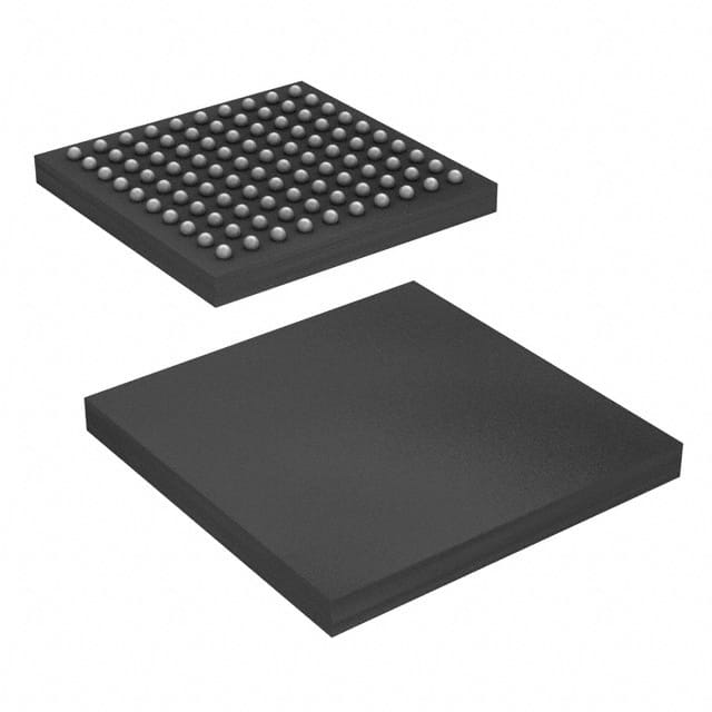
- Part No.:
- CYP15G0101DXB-BBI
- Manufacturer:
- Infineon Technologies
- Category:
- Telecom
- Package:
- 100-LBGA
- Datasheet:
-
 CYP15G0101DXB-BBI.pdf
- Description:
- IC TELECOM INTERFACE 100TBGA
- Quantity:
- Payment:

- Shipping:

Inventory:3,532
Please send an inquiry. Send us your inquiry, and we will respond immediately.
Product details
Overview
CYP15G0101DXB-BBI from Cypress Semiconductor Corporation is a single-channel HOTLink II™ transceiver IC for high-speed point-to-point serial data transmission over fiber, copper, or PCB traces. It operates at 195–1500 MBaud serial data rate, supports 8B/10B encoding or 10-bit unencoded mode, features dual PECL-compatible differential I/O, and delivers 1.25W typical power consumption at 3.3V - deployed in video transmission systems and telecom base-station backplanes.
For engineers reviewing the CYP15G0101DXB-BBI datasheet, CYP15G0101DXB-BBI pinout, CYP15G0101DXB-BBI application, or CYP15G0101DXB-BBI equivalent, key selection considerations include its SMPTE-noncompliant data-rate range (vs. CYV/CYW variants), selectable parity generation/checking, internal PLL clock synchronization, and JTAG boundary-scan support for at-speed link validation.
Technical Context
The CYP15G0101DXB-BBI implements a fully integrated transmit/receive channel with independent PLL-based clock recovery and synthesis: TX uses a 10× or 20× REFCLK multiplier (selected by TXRATE), while RX employs a clock-and-data-recovery (CDR) PLL with no external components. Its MultiFrame™ Receive Framer provides bit- and byte-level alignment with K28.5 comma detection and configurable framer depth.
It supports synchronous LVTTL parallel I/O with flexible clocking options: TX can be clocked by REFCLK or TXCLK (via TXCKSEL), and RX output timing may reference recovered clock (RXCKSEL = MID/HIGH) or local REFCLK (RXCKSEL = LOW). The Elasticity Buffer (RX path) and Phase-Align Buffer (TX path) are optional and configurable via control pins.
Key Specifications
| Parameter | Value and Actual Design Meaning |
|---|---|
| Serial Data Rate | 195–1500 MBaud - defines usable signaling bandwidth for ESCON®, DVB-ASI, Fibre Channel, and Gigabit Ethernet links. |
| Encoding Mode | 8B/10B encoded or 10-bit unencoded - enables compatibility with legacy protocols requiring raw data transport or standard-compliant framing. |
| Supply Voltage | 3.3V ±5% - single-rail operation simplifies power delivery and eliminates level-shifting on parallel interface. |
| Power Dissipation | 1.25W typical - measured at full-rate operation; enables thermal management in dense backplane designs. |
| Input/Output Interface | LVTTL parallel (8-bit + control) / PECL-compatible differential serial - ensures interoperability with FPGA I/O banks and optical module drivers. |
| Compliance | CPRI™ compliant; non-SMPTE 259M/292M and non-OBSAI-RP3 - distinguishes it from CYV/CYW variants for general-purpose high-speed serial interconnects. |
| JTAG Support | Built-in boundary scan (IEEE 1149.1) - enables board-level testability without external probing of high-speed serial lanes. |
Pinout & Package
Package: 100-ball BGA, Pb-free option available, 0.25µm BiCMOS process.
| Pin/Terminal | Circuit Role | Design Meaning |
|---|---|---|
| TXD[7:0] | Parallel data input | Synchronous LVTTL inputs sampled by TXCLK or REFCLK; carry 8-bit characters to encoder or shifter. |
| IN1±, IN2± | Differential serial receive inputs | PECL-compatible inputs with internal DC restoration; accept serial bitstream from optical/copper media. |
| OUT1±, OUT2± | Differential serial transmit outputs | Source-matched 50Ω drivers; no external bias resistors required; edge rates controlled by signaling rate. |
| RXD[7:0] | Parallel data output | LVTTL outputs presenting decoded, framed characters to host system; synchronized to RXCLK± or REFCLK. |
| TXCLKO± | Transmit character clock output | True/complement LVTTL clock derived from TX PLL; frequency = REFCLK (TXRATE=LOW) or 2×REFCLK (TXRATE=HIGH). |
| RXST[2:0] | Receive status indicator | 3-bit LVTTL output indicating framer lock, alignment state, and error conditions per MultiFrame™ logic. |
Key Features
| Feature | Design Value |
|---|---|
| MultiFrame™ Receive Framer | Enables both bit- and byte-aligned recovery with K28.5 detection and selectable framer depth - critical for deterministic latency in video transport. |
| Optional Elasticity Buffer (RX) | Compensates for clock domain mismatches between recovered and system clocks - essential for jitter-tolerant reception in asynchronous links. |
| Phase-Align Buffer (TX) | Adjusts phase relationship between parallel input clock and internal character clock - prevents metastability during clock domain crossing. |
| Built-In Self-Test (BIST) | At-speed link testing with pattern generator/checker - validates physical layer integrity without external test equipment. |
| Per-channel Link Quality Indicator | Analog signal detect + digital signal detect outputs - enables real-time link health monitoring in field-deployed systems. |
Applications
| Video Backhaul Transmission | Base-Station Interconnect |
|---|---|
Use Scenario: Transmitting uncompressed HD-SDI or 3G-SDI video streams across backplane or fiber links between camera processing units and distribution switches. IC Role / Device Role / Timing Role: Serializes parallel pixel data, performs 8B/10B encoding, recovers embedded clock, and maintains low-latency framing for real-time video. Use Value: Eliminates wide parallel buses, reduces EMI, and supports >1 Gbps throughput with deterministic jitter performance. | Use Scenario: Connecting RF processing modules to baseband units in LTE/5G macro base stations using CPRI-compliant serial interfaces. IC Role / Device Role / Timing Role: Acts as CPRI-compliant transceiver handling IQ sample transport at 1.2288 Gbps or 2.4576 Gbps with precise timing recovery. Use Value: Enables deterministic latency and frame alignment required for coordinated multi-point (CoMP) and MIMO processing. |
| Network Switch Fabric Interface | High-Speed Test Equipment |
Use Scenario: Replacing parallel bus interconnects between line cards and switch fabric ASICs in enterprise/core routers. IC Role / Device Role / Timing Role: Provides point-to-point serial link with built-in framer and elasticity buffer to absorb clock skew across modular chassis. Use Value: Increases per-lane bandwidth while reducing connector count and improving signal integrity over long PCB traces. | Use Scenario: Embedded in automated test equipment (ATE) for validating high-speed serial PHYs using programmable BIST patterns. IC Role / Device Role / Timing Role: Generates and checks at-speed PRBS or custom patterns across optical/copper links with JTAG-controlled diagnostics. Use Value: Reduces dependency on external pattern generators and enables in-system validation of link margin and BER. |
Equivalent & Alternatives
The following parts are listed as comparable options for similar high-speed serial transceiver applications.
| Alternative Part | Technical Difference | Application Difference | Selection Advice |
|---|---|---|---|
| CYV15G0101DXB | SMPTE 259M/292M compliant; passes EG34-1999 pathological tests; identical pinout and package. | Required for broadcast video equipment certified to SMPTE standards. | Select when compliance with SMPTE 259M/292M pathological test requirements is mandatory. |
| CYW15G0101DXB | OBSAI-RP3 compliant; supports 1536/768 MBaud rates; identical pinout and package. | Targeted at legacy OBSAI-based wireless infrastructure deployments. | Select only if interfacing with OBSAI-RP3-defined baseband units or legacy radio units. |
Compared with CYV15G0101DXB and CYW15G0101DXB, the CYP15G0101DXB-BBI offers broader general-purpose serial interconnect capability without SMPTE or OBSAI certification overhead - ideal for cost-sensitive, non-standardized high-speed links where full protocol compliance is not required.
Availability
CYP15G0101DXB-BBI is available at Aetrix Electronics and suitable for video backhaul transmission, base-station interconnect, and network switch fabric interface requiring stable component supply, long-term lifecycle support, and traceable sourcing.
Supply support for CYP15G0101DXB-BBI includes scheduled delivery planning, volume procurement assistance, BOM continuity management, traceable sourcing, and lifecycle availability coordination for OEM customers, industrial embedded developers, connected-device designers, and electronics production programs.
Manufacturer
Cypress Semiconductor Corporation, now part of Infineon Technologies, designs high-performance mixed-signal ICs for connectivity, memory, and programmable solutions.
The HOTLink II™ transceiver product line targets high-speed serial interconnect in telecom, broadcast video, and test equipment - emphasizing protocol flexibility, embedded clock recovery, and system-level diagnostic capability.
FAQ
What is the difference between CYP15G0101DXB-BBI and CYV15G0101DXB?
CYP15G0101DXB-BBI is not compliant with SMPTE 259M/292M pathological test requirements, whereas CYV15G0101DXB is verified to pass all EG34-1999 test patterns. Both share identical pinout, package, and core functionality, but CYV is mandated for broadcast-grade SDI/HD-SDI equipment certification.
Does CYP15G0101DXB-BBI require external termination resistors on PECL serial I/O?
No. The device integrates source-matched 50Ω drivers for OUT1±/OUT2± and internal DC restoration for IN1±/IN2±, eliminating need for external biasing or termination resistors - simplifying PCB layout and reducing bill-of-materials.
Can the 8B/10B encoder/decoder be bypassed in CYP15G0101DXB-BBI?
Yes. The encoder/decoder is fully bypassable via TXMODE[1] control; when disabled, the device transports raw 10-bit parallel data across the serial link - enabling use with externally scrambled or pre-encoded protocols like CPRI or proprietary baseband formats.
How is clock domain crossing handled between parallel and serial interfaces?
Through two dedicated buffers: the Phase-Align Buffer (TX path) dynamically adjusts phase alignment between parallel input clock and internal character clock, while the Elasticity Buffer (RX path) absorbs frequency/phase differences between recovered clock and system clock - ensuring reliable data transfer across asynchronous domains.
CYP15G0101DXB-BBI Specifications
- Product attributes
- Attribute value
- Manufacturer:
- Infineon Technologies
- Series:
- HOTlink II™
- Package/Case:
- 100-LBGA
- Packaging:
- Tray
- Product Status:
- Obsolete
- Function:
- Transceiver
- Interface:
- LVTTL
- Number of Circuits:
- -
- Voltage - Supply:
- 3.135V ~ 3.465V
- Current - Supply:
- 390mA
- Power (Watts):
- -
- Operating Temperature:
- -40°C ~ 85°C
- Grade:
- -
- Qualification:
- -
- Mounting Type:
- Surface Mount
- Supplier Device Package:
- 100-TBGA (11x11)
CYP15G0101DXB-BBI FAQ
1.How can I place an order for CYP15G0101DXB-BBI through Aetrix?
Please submit a Request for Quotation (RFQ) for CYP15G0101DXB-BBI on Aetrix. Our sales agent will provide a competitive quotation and guide you through the order confirmation once you accept the terms.
2.Are the price and stock information for CYP15G0101DXB-BBI reliable?
The price and inventory of CYP15G0101DXB-BBI are updated periodically and may fluctuate due to market conditions. Stock and pricing data are typically refreshed every 24 hours. Quotation validity for CYP15G0101DXB-BBI is usually 5 days.
3.What payment methods are accepted for CYP15G0101DXB-BBI?
We accept Wire Transfer, PayPal, Credit Card, Western Union, MoneyGram, and Escrow for CYP15G0101DXB-BBI transactions.
Note: Certain payment methods may incur a processing fee.
4.How is shipping managed for CYP15G0101DXB-BBI?
CYP15G0101DXB-BBI orders can be shipped via leading logistics carriers, including DHL, UPS, FedEx, TNT, or Registered Mail.
Once your CYP15G0101DXB-BBI order is processed, you will receive an email with the shipment details and tracking number.
Note: Tracking information may take up to 24 hours to appear. Express delivery typically takes 3–5 business days.
5.How can I obtain technical support or documentation for CYP15G0101DXB-BBI?
For technical support, including CYP15G0101DXB-BBI datasheets, pinout diagrams, or application guidance, please contact our engineering support team. They can provide detailed documentation and assistance for your CYP15G0101DXB-BBI requirements.
6.How does Aetrix verify that CYP15G0101DXB-BBI is sourced from the original manufacturer or authorized distributors?
All CYP15G0101DXB-BBI products on Aetrix are procured from qualified distributors and authorized channels. Our dedicated quality assurance team conducts strict verification, including traceability checks and, if necessary, third-party testing. This ensures that CYP15G0101DXB-BBI meets industry standards.
7.What is the process for return or replacement of CYP15G0101DXB-BBI?
All CYP15G0101DXB-BBI units undergo pre-shipment inspection (PSI). If there is an issue with CYP15G0101DXB-BBI, returns or replacements are accepted under the following conditions:
1.Quantity discrepancies, incorrect items, or visible external defects (such as breakage or corrosion), acknowledged by Aetrix.
2.The issue is reported within 90 days of delivery.
3.The CYP15G0101DXB-BBI part is unused and in its original packaging.
Return procedure for CYP15G0101DXB-BBI:
1.Submit a request within 90 days.
2.Obtain a Return Material Authorization (RMA) from Aetrix.
CYP15G0101DXB-BBI Tags

-
LMC567CMX/NOPB
Texas Instruments
-
LM567CMX/NOPB
Texas Instruments
-
LM567CM/NOPB
Texas Instruments

-
VSC8531XMW-02
Microchip Technology
-
VSC8531XMW-05
Microchip Technology

-
GPY115C0VI
MaxLinear, Inc.

-
SI32185-A-FMR
Skyworks Solutions Inc.

-
VSC8541XMV-05
Microchip Technology

-
SI32178-B-FM1R
Skyworks Solutions Inc.
-
GPY215C0VI
MaxLinear, Inc.

-
CPC7514ZTR
Littelfuse Inc.

-
VSC8502XML-03
Microchip Technology
Tech Hub

An engineering guide to LED driver operation, constant-current and constant-voltage outputs, linear and switching topologies, dimming, IC selection, calculations, replacement compatibility, and fault c…

Operational amplifier guide covering op amp basics, feedback, ideal vs real op amps, common configurations, buffer circuits, offset, bias current, gain-bandwidth, slew rate, rail-to-rail limits and sel…

Jumper cables guide covering safe connection order, red and black clamp placement, final ground connection, cable gauge, length, clamp quality, copper vs CCA cables, jump starter comparison and battery…

LDO regulator guide covering low dropout voltage, power dissipation, thermal design, PSRR, output noise, capacitor stability, adjustable LDO circuits, LDO vs buck converter and datasheet selection chec…

Conditional Access Module guide covering CAM meaning, CI/CI+ interface, smart card authorization, DVB security workflow, TV and set-top box compatibility, internal electronics, ESD protection, connecto…

Guide to electronic component obsolescence covering EOL risk, PCN/PDN notices, last-time buy planning, replacement options, form-fit-function validation, counterfeit risk and BOM lifecycle management.

18650 battery guide covering lithium-ion cell basics, 3.6V/3.7V voltage, 4.2V charging, mAh and Wh capacity, protected cells, chargers, BMS, series-parallel packs, holders, welding and sourcing checks.…

Hall effect sensor guide covering working principle, linear and digital sensors, Arduino circuits, current sensing, speed detection, automotive applications, A3144 examples, signal filtering and datash…

Product Change Notification guide for electronic components, covering PCN meaning, PCN vs PDN/EOL, common change types, risk levels, form-fit-function review, engineering validation, BOM control, LTB/L…

A practical guide to blend door actuators, covering HVAC function, symptoms, location, AC and heater issues, reset and calibration, replacement cost, electrical diagnosis, compatibility checks, and rep…


