
 My Inquiry
 My Account


Infineon Technologies CYV15G0204TRB-BGC
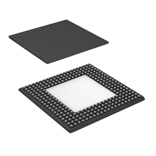
- Part No.:
- CYV15G0204TRB-BGC
- Manufacturer:
- Infineon Technologies
- Category:
- Serializers, Deserializers
- Package:
- 256-BGA Exposed Pad
- Datasheet:
-
 CYV15G0204TRB-BGC.pdf
- Description:
- IC SERDES HOTLINK 256LBGA
- Quantity:
- Payment:

- Shipping:

Inventory:2,615
Please send an inquiry. Send us your inquiry, and we will respond immediately.
Product details
Overview
CYV15G0204TRB from Cypress Semiconductor Corporation is a second-generation HOTLink II™ dual serializer and dual reclocking deserializer IC for SMPTE 259M/292M video applications. It provides independent 195–1500 Mbps serial links per channel, supports simultaneous full/half-rate operation at different signaling rates (e.g., 1.485 Gbps and 1.485/1.001 Gbps), and integrates PLLs with no external components. Used in multi-format SDI routers and camera control units.
For engineers reviewing the CYV15G0204TRB datasheet, CYV15G0204TRB pinout, CYV15G0204TRB application, or CYV15G0204TRB equivalent, key selection criteria include dual-channel rate independence, integrated CDR PLLs, PECL-compatible differential I/O with internal termination, BIST-enabled at-speed link validation, and SMPTE compliance without external clock conditioning.
Technical Context
The CYV15G0204TRB implements two fully independent transmit channels (TXA/TXB) and two independent receive/reclocker channels (RXC/RXD), each with dedicated PLLs, phase-align buffers, and BIST engines. Each TX channel accepts 10-bit LVTTL parallel data synchronized to REFCLKx± or TXCLKx and serializes at 10× or 20× that rate.
Each RX channel employs a fully integrated Clock and Data Recovery (CDR) PLL to reconstruct timing from PECL-compatible differential inputs (INC1±/INC2±), then deserializes to 10-bit parallel outputs (RXDC[9:0]/RXDD[9:0]) while simultaneously reclocking and retransmitting via ROUTC1±/ROUTC2± and ROUTD1±/ROUTD2±.
Key Specifications
| Parameter | Value and Actual Design Meaning |
|---|---|
| Serial Data Rate | 195–1500 Mbps per link - enables SD/HD/3G-SDI transport without retiming bottlenecks |
| Input Interface | 10-bit LVTTL parallel - synchronous capture with REFCLKx± or TXCLKx, supporting half/full-rate clocking |
| Output Interface | Differential PECL-compatible serial - internally terminated, no external bias resistors required |
| CDR Architecture | Fully integrated PLL-based CDR per RX channel - eliminates need for external clock recovery ICs |
| Power Consumption | 2.5W typical at 3.3V - optimized for thermally constrained broadcast equipment chassis |
| Compliance | SMPTE 259M & 292M compliant per EG34-1999 pathological test - validated for broadcast-grade signal integrity |
| Built-in Test | Per-channel BIST with LFSR pattern generation/checking - enables at-speed production testing of serial links |
Pinout & Package
Package: 20×20 mm thermally enhanced Pb-free BGA (196-ball, 0.8 mm pitch).
| Pin/Terminal | Circuit Role | Design Meaning |
|---|---|---|
| REFCLKA±, REFCLKB± | Differential reference clock input | Timing reference for TX PLLs; supports LVPECL or single-ended LVTTL; determines character rate |
| TXDA[9:0], TXDB[9:0] | LVTTL parallel data input | 10-bit synchronous input per channel; sampled on rising edge of REFCLKx± or TXCLKx |
| TOUTA1±, TOUTA2±, TOUTB1±, TOUTB2± | Differential PECL serial output | Redundant serialized outputs per TX channel; internally terminated; edge-rate controlled by signaling rate |
| INC1±, INC2±, IND1±, IND2± | Differential PECL serial input | Selectable differential inputs per RX channel; feed CDR PLL for clock recovery and data reconstruction |
| ROUTC1±, ROUTC2±, ROUTD1±, ROUTD2± | Differential PECL reclocked output | Reclocked serial retransmission outputs; preserve recovered timing; no external components needed |
| RXDC[9:0], RXDD[9:0] | LVTTL parallel data output | 10-bit deserialized output per RX channel; synchronous to recovered RXCLKC±/RXCLKD± |
| TRGCLKC±, TRGCLKD± | Reclocker trigger clock output | Recovered character-rate clocks for downstream logic synchronization; derived from CDR PLL |
Key Features
| Feature | Design Value |
|---|---|
| Independent dual-channel operation | Each TX/RX pair operates at different signaling rates (e.g., 1.485 Gbps + 1.001 Gbps) without cross-talk or shared clock constraints |
| Integrated CDR with no external components | Eliminates discrete clock recovery ICs and associated loop-filter passives, reducing board area and BOM count |
| Internal DC restoration | Maintains baseline stability on AC-coupled PECL links without external bias networks or capacitors |
| JTAG boundary scan | Enables IEEE 1149.1-compliant interconnect testing and configuration verification in-system |
| Link Quality Indicator (LQI) | Separate analog signal detect and digital signal detect outputs provide real-time link health monitoring |
Applications
| Multi-Format SDI Router | HD Camera Control Unit |
|---|---|
|
Use Scenario: Routing SMPTE 259M (270 Mbps) and SMPTE 292M (1.485 Gbps) video streams between multiple sources and destinations. IC Role / Device Role / Timing Role: Dual serializer/deserializer bridges parallel video processors to serial backplane links with independent rate handling per port. Use Value: Enables single-chip support for mixed SD/HD formats without external rate-matching FIFOs or clock domain crossing logic. |
Use Scenario: Transmitting uncompressed HD-SDI video and bidirectional control data (RS-422, GPIO) from camera head to base station. IC Role / Device Role / Timing Role: Serializer converts parallel sensor data to robust 1.485 Gbps serial; deserializer reclocks incoming control commands. Use Value: Maintains jitter < 0.3 UI over 100 m coaxial cable using integrated CDR and PECL drivers, meeting SMPTE 292M eye mask requirements. |
| SDI Format Converter | Professional SDI Monitor |
|
Use Scenario: Converting between 3G-SDI (2.97 Gbps) baseband and dual-link HD-SDI (2 × 1.485 Gbps) for legacy infrastructure compatibility. IC Role / Device Role / Timing Role: Deserializes incoming 3G-SDI (via two CYV15G0204TRB channels in parallel), processes, then reserializes as dual-link HD-SDI. Use Value: Supports simultaneous 195–1500 Mbps operation per channel, enabling precise alignment of dual-link timing without external delay calibration. |
Use Scenario: Real-time display of embedded audio, ancillary data, and video timing signals from broadcast feeds. IC Role / Device Role / Timing Role: Reclocking deserializer ensures clean, low-jitter pixel clock recovery for frame-synchronized video processing. Use Value: Integrated Link Quality Indicator provides immediate detection of signal degradation before visible artifacts appear on screen. |
Equivalent & Alternatives
The following parts are listed as comparable options for similar dual-channel high-speed video serializer/deserializer applications.
| Alternative Part | Technical Difference | Application Difference | Selection Advice |
|---|---|---|---|
| TI TLK2711 | Single-channel 1.5–3.125 Gbps SerDes; no integrated reclocker outputs; requires external CDR for retransmission | Targeted at point-to-point fiber links, not multi-channel SMPTE routing | Choose when only one high-speed link is needed and reclocking is handled externally |
| Maxim MAX9205/MAX9206 | LVDS-based (not PECL); max 622 Mbps; no SMPTE 292M compliance; lower power (1.2W) | Designed for automotive camera links, not broadcast video infrastructure | Choose for cost-sensitive, lower-data-rate automotive vision systems with LVDS interface preference |
Compared with TLK2711 and MAX9205/MAX9206, the CYV15G0204TRB uniquely delivers dual independent SMPTE-compliant channels with integrated reclocking, eliminating external CDRs and enabling true multi-standard video infrastructure in a single package.
Availability
CYV15G0204TRB is available at Aetrix Electronics and suitable for SMPTE 259M/292M video routers, HD camera control units, SDI format converters, and professional broadcast monitors requiring stable component supply across extended product lifecycles.
Supply support for CYV15G0204TRB includes scheduled delivery planning, volume procurement assistance, BOM continuity management, traceable sourcing, and lifecycle availability coordination for OEM customers, industrial embedded developers, connected-device designers, and electronics production programs.
Manufacturer
Cypress Semiconductor Corporation, now part of Infineon Technologies, designs high-performance mixed-signal ICs for communications, computing, and industrial markets.
The CYV15G0204TRB belongs to the HOTLink II™ family, engineered specifically for SMPTE-compliant broadcast video infrastructure requiring deterministic low-latency serialization, reclocking, and interoperability across mixed data rates.
FAQ
What clocking configurations does CYV15G0204TRB support for independent channel operation?
The device supports full-rate (REFCLKx± = character rate) and half-rate (REFCLKx± = half-character rate) modes per channel. Each TX/RX channel uses its own REFCLKx±, allowing simultaneous operation at different rates-e.g., REFCLKA± at 148.5 MHz (1.485 Gbps) and REFCLKB± at 100.1 MHz (1.001 Gbps). TXCKSELx selects whether REFCLKx± or TXCLKx drives the parallel interface.
How does the built-in Link Quality Indicator (LQI) function in real-world deployment?
LQI provides two independent outputs: analog signal detect (ASD) asserts when valid differential amplitude (>100 mVpp) is present, and digital signal detect (DSD) asserts only when both valid amplitude and correct data transition density are confirmed. This enables early warning of marginal cable or connector degradation before bit errors occur, critical for broadcast uptime.
Can CYV15G0204TRB operate with single-ended LVTTL reference clocks instead of differential PECL?
Yes. REFCLKA± and REFCLKB± accept single-ended LVTTL inputs: connect the clock source to either REFCLKx+ or REFCLKx− and leave the complementary pin floating. The internal receiver automatically adapts. However, differential LVPECL is recommended for noise immunity in high-density video chassis environments.
What is the role of the Phase-Align Buffer (PAB) and how is it managed during dynamic rate changes?
The PAB absorbs phase drift between REFCLKx± and TXCLKx. When TXCLKx phase shifts beyond ±180°, TXERRx asserts. To recover, write PABRSTx = 0 via the configuration interface-this resets the buffer and reinitializes alignment. This mechanism enables seamless switching between asynchronous clock domains without data loss or manual resynchronization.
CYV15G0204TRB-BGC Specifications
- Product attributes
- Attribute value
- Manufacturer:
- Infineon Technologies
- Series:
- -
- Package/Case:
- 256-BGA Exposed Pad
- Packaging:
- Tray
- Product Status:
- Obsolete
- Function:
- Serializer/Deserializer
- Data Rate:
- 1.485Gbps
- Input Type:
- LVTTL
- Output Type:
- PECL
- Number of Inputs:
- 20/4
- Number of Outputs:
- 4/20
- Voltage - Supply:
- 3.3V
- Operating Temperature:
- 0°C ~ 70°C (TA)
- Grade:
- -
- Qualification:
- -
- Mounting Type:
- Surface Mount
- Supplier Device Package:
- 256-L2BGA (27x27)
CYV15G0204TRB-BGC FAQ
1.How can I place an order for CYV15G0204TRB-BGC through Aetrix?
Please submit a Request for Quotation (RFQ) for CYV15G0204TRB-BGC on Aetrix. Our sales agent will provide a competitive quotation and guide you through the order confirmation once you accept the terms.
2.Are the price and stock information for CYV15G0204TRB-BGC reliable?
The price and inventory of CYV15G0204TRB-BGC are updated periodically and may fluctuate due to market conditions. Stock and pricing data are typically refreshed every 24 hours. Quotation validity for CYV15G0204TRB-BGC is usually 5 days.
3.What payment methods are accepted for CYV15G0204TRB-BGC?
We accept Wire Transfer, PayPal, Credit Card, Western Union, MoneyGram, and Escrow for CYV15G0204TRB-BGC transactions.
Note: Certain payment methods may incur a processing fee.
4.How is shipping managed for CYV15G0204TRB-BGC?
CYV15G0204TRB-BGC orders can be shipped via leading logistics carriers, including DHL, UPS, FedEx, TNT, or Registered Mail.
Once your CYV15G0204TRB-BGC order is processed, you will receive an email with the shipment details and tracking number.
Note: Tracking information may take up to 24 hours to appear. Express delivery typically takes 3–5 business days.
5.How can I obtain technical support or documentation for CYV15G0204TRB-BGC?
For technical support, including CYV15G0204TRB-BGC datasheets, pinout diagrams, or application guidance, please contact our engineering support team. They can provide detailed documentation and assistance for your CYV15G0204TRB-BGC requirements.
6.How does Aetrix verify that CYV15G0204TRB-BGC is sourced from the original manufacturer or authorized distributors?
All CYV15G0204TRB-BGC products on Aetrix are procured from qualified distributors and authorized channels. Our dedicated quality assurance team conducts strict verification, including traceability checks and, if necessary, third-party testing. This ensures that CYV15G0204TRB-BGC meets industry standards.
7.What is the process for return or replacement of CYV15G0204TRB-BGC?
All CYV15G0204TRB-BGC units undergo pre-shipment inspection (PSI). If there is an issue with CYV15G0204TRB-BGC, returns or replacements are accepted under the following conditions:
1.Quantity discrepancies, incorrect items, or visible external defects (such as breakage or corrosion), acknowledged by Aetrix.
2.The issue is reported within 90 days of delivery.
3.The CYV15G0204TRB-BGC part is unused and in its original packaging.
Return procedure for CYV15G0204TRB-BGC:
1.Submit a request within 90 days.
2.Obtain a Return Material Authorization (RMA) from Aetrix.
CYV15G0204TRB-BGC Tags

-
SN65HVS880PWPR
Texas Instruments
-
SN65HVS882PWPR
Texas Instruments

-
FIN3386MTDX
onsemi
-
FIN3385MTDX
onsemi

-
SN65LV1023ARHBR
Texas Instruments

-
SN65LV1023ADBR
Texas Instruments
-
SN65LV1224BDBR
Texas Instruments

-
SN65LVDS93ADGGR
Texas Instruments
-
SN65LVDS93DGGR
Texas Instruments

-
TDES954RGZT
Texas Instruments
-
SN65LV1224BRHBT
Texas Instruments

-
DS90UB914QSQE/NOPB
Texas Instruments
Tech Hub

An engineering guide to LED driver operation, constant-current and constant-voltage outputs, linear and switching topologies, dimming, IC selection, calculations, replacement compatibility, and fault c…

Operational amplifier guide covering op amp basics, feedback, ideal vs real op amps, common configurations, buffer circuits, offset, bias current, gain-bandwidth, slew rate, rail-to-rail limits and sel…

Jumper cables guide covering safe connection order, red and black clamp placement, final ground connection, cable gauge, length, clamp quality, copper vs CCA cables, jump starter comparison and battery…

LDO regulator guide covering low dropout voltage, power dissipation, thermal design, PSRR, output noise, capacitor stability, adjustable LDO circuits, LDO vs buck converter and datasheet selection chec…

Conditional Access Module guide covering CAM meaning, CI/CI+ interface, smart card authorization, DVB security workflow, TV and set-top box compatibility, internal electronics, ESD protection, connecto…

Guide to electronic component obsolescence covering EOL risk, PCN/PDN notices, last-time buy planning, replacement options, form-fit-function validation, counterfeit risk and BOM lifecycle management.

18650 battery guide covering lithium-ion cell basics, 3.6V/3.7V voltage, 4.2V charging, mAh and Wh capacity, protected cells, chargers, BMS, series-parallel packs, holders, welding and sourcing checks.…

Hall effect sensor guide covering working principle, linear and digital sensors, Arduino circuits, current sensing, speed detection, automotive applications, A3144 examples, signal filtering and datash…

Product Change Notification guide for electronic components, covering PCN meaning, PCN vs PDN/EOL, common change types, risk levels, form-fit-function review, engineering validation, BOM control, LTB/L…

A practical guide to blend door actuators, covering HVAC function, symptoms, location, AC and heater issues, reset and calibration, replacement cost, electrical diagnosis, compatibility checks, and rep…


