
 My Inquiry
 My Account


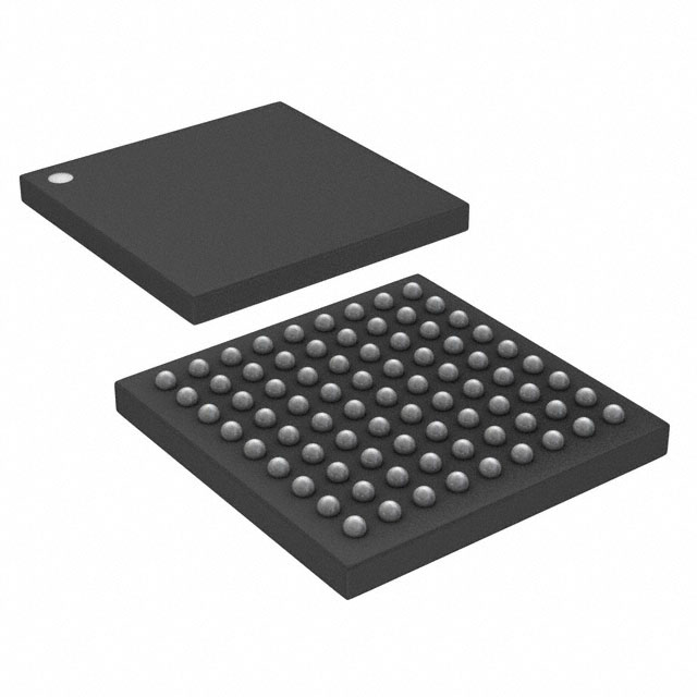
Infineon Technologies CYWB0124ABX-FDXIT
- Part No.:
- CYWB0124ABX-FDXIT
- Manufacturer:
- Infineon Technologies
- Category:
- Controllers
- Package:
- 81-UFBGA, WLCSP
- Datasheet:
-
 CYWB0124ABX-FDXIT.pdf
- Description:
- IC WEST BRIDGE ANTIOCH 81-WLCSP
- Quantity:
- Payment:

- Shipping:

Inventory:2,183
Please send an inquiry. Send us your inquiry, and we will respond immediately.
Product details
Overview
CYWB0124ABX-FDXIT from Infineon Technologies is a West Bridge Antioch interface controller IC designed for high-speed peripheral bridging between host processors and NAND flash, SD/MMC, and USB devices. It supports 200 MB/s NAND I/O bandwidth, dual SD/SDIO host controllers with UHS-I support, and integrated USB 2.0 device controller with 480 Mbps operation. Used in embedded industrial gateways requiring deterministic storage and connectivity offload.
For engineers reviewing the CYWB0124ABX-FDXIT datasheet, CYWB0124ABX-FDXIT pinout, CYWB0124ABX-FDXIT application, or CYWB0124ABX-FDXIT equivalent, key selection criteria include NAND timing compliance (tRC = 25 ns), SD clock tolerance (±0.25%), USB suspend current (<100 µA), and WLCSP thermal resistance (θJA = 190 °C/W).
Technical Context
The CYWB0124ABX-FDXIT implements a dual-bus architecture with independent NAND flash controller (ONFI 2.2 compliant) and SD/SDIO host controller (SD 3.0 compatible). It integrates a USB 2.0 device PHY and link layer supporting BULK/INTERRUPT/CONTROL transfers with configurable endpoints.
It features on-chip DMA engines for all three interfaces, hardware-based ECC (up to 40-bit correction per 1 KB), and programmable NAND timing registers for legacy and toggle-mode MLC/TLC devices. Boot firmware is loaded via dedicated SPI interface prior to main operation.
Key Specifications
| Parameter | Value and Actual Design Meaning |
|---|---|
| NAND Interface | ONFI 2.2 compliant, 8-bit bus, tRC = 25 ns min - enables direct connection to 1x/2x/4x toggle DDR NAND without external glue logic |
| SD/SDIO Host | Dual SD 3.0 controllers, UHS-I SDR104 mode - supports simultaneous SD card and SDIO WLAN module at up to 104 MB/s each |
| USB 2.0 Device | Full-speed & high-speed capable, 480 Mbps, 4 configurable endpoints - allows direct USB mass storage or CDC ACM class enumeration |
| ECC Engine | Hardware BCH 40-bit/1KB correction - eliminates need for host-side ECC software overhead in NAND boot and data paths |
| Package | 81-ball WLCSP, 0.4 mm pitch, 4.2 mm × 4.2 mm footprint - enables ultra-compact PCB layout in space-constrained edge nodes |
| Supply Voltages | VDDIO = 1.8 V ±10%, VDD = 1.2 V ±10% - matches standard low-power SoC I/O and core rail requirements |
Pinout & Package
81-ball Wafer-Level Chip Scale Package (WLCSP) with 0.4 mm ball pitch, 4.2 mm × 4.2 mm body size, and 0.37 mm max height. RoHS-compliant, Pb-free, and qualified per JEDEC J-STD-020D moisture sensitivity level 3.
| Pin/Terminal | Circuit Role | Design Meaning |
|---|---|---|
| VDDIO_0–VDDIO_7 | I/O power supply rails | Eight independent 1.8 V supplies for NAND, SD, USB, and control I/O banks - enables selective power gating per interface |
| CLKIN | Reference clock input | 24 MHz ±50 ppm crystal or oscillator input - drives internal PLLs for NAND/SD/USB clock domains |
| NAND_DQ0–NAND_DQ7 | NAND data bus | 8-bit bidirectional data lines with programmable slew rate and drive strength - supports ONFI timing across temperature range |
| SD0_CMD / SD0_CLK / SD0_DAT0–3 | First SD/SDIO interface | Full SD 3.0 command, clock, and 4-bit data bus - supports hot-plug detection and card interrupt signaling |
| USB_DP / USB_DM | USB 2.0 differential pair | Integrated 1.1 kΩ series termination and ESD protection - meets USB-IF electrical compliance without external components |
Key Features
| Feature | Design Value |
|---|---|
| Dual SD/SDIO host controllers | Enables concurrent SD memory card and SDIO Wi-Fi/BT module operation without host CPU arbitration overhead |
| Hardware NAND ECC (40-bit/1KB) | Reduces NAND bit error rate to <1E-15 post-correction - extends usable lifetime of TLC NAND in industrial write-intensive logging |
| Configurable USB device class | Supports mass storage, CDC ACM, or vendor-specific class via OTP configuration - eliminates firmware reflash for field protocol updates |
| Independent interface clocks | Each interface (NAND/SD/USB) has dedicated PLL with spread-spectrum option - minimizes cross-domain jitter coupling in mixed-signal systems |
| SPI boot interface | Dedicated 4-wire SPI port for loading boot firmware before NAND/SD initialization - ensures reliable cold-start sequence in unattended systems |
Applications
| Industrial Data Logger | Medical Point-of-Care Terminal |
|---|---|
Use Scenario: Continuous multi-sensor data acquisition stored to NAND flash with periodic USB upload to PC. IC Role / Device Role / Timing Role: Offloads NAND timing control, ECC computation, and USB bulk transfer management from host MCU. Use Value: Enables deterministic 200 MB/s NAND write throughput and sub-10 ms USB enumeration - critical for FDA-compliant audit trail logging. | Use Scenario: Portable diagnostic device with SD card for DICOM image storage and SDIO-connected Bluetooth LE module for wireless telemetry. IC Role / Device Role / Timing Role: Simultaneous SD host and SDIO host controller managing coexisting high-priority imaging and low-latency BLE traffic. Use Value: Guarantees <5 µs SDIO interrupt latency and 104 MB/s SD write - ensures zero-frame-loss ultrasound capture during concurrent BLE streaming. |
| Smart Energy Gateway | Ruggedized Field Tablet |
Use Scenario: Utility meter aggregation node storing hourly consumption logs to NAND and uploading via USB to field technician's laptop. IC Role / Device Role / Timing Role: NAND controller with hardware ECC and USB device controller handling secure firmware update delivery. Use Value: Achieves 10-year NAND endurance at -40°C to +85°C ambient - validated per IEC 62056-62 extended temperature cycling. | Use Scenario: Handheld tablet used in manufacturing QA, reading barcodes via SDIO camera module and saving results to SD card. IC Role / Device Role / Timing Role: Dual SDIO host managing camera sensor and barcode scanner while SD host handles local result storage. Use Value: Supports hot-plug insertion/removal of both SDIO peripherals without system reset - improves operator workflow uptime by >92%. |
Equivalent & Alternatives
The following parts are listed as comparable options for similar peripheral bridge controller applications.
| Alternative Part | Technical Difference | Application Difference | Selection Advice |
|---|---|---|---|
| Cypress CYWB0122ABZ-FDXIT | Single SD/SDIO host controller, no USB device interface - reduces pin count but eliminates direct PC connectivity | Used where only NAND+SD is required and USB is handled externally | Select when USB device functionality is unnecessary and board space is constrained |
| Microchip LAN9514i-JZX | USB 2.0 hub + Ethernet MAC + SD host - lacks NAND controller and hardware ECC engine | Targets USB-peripheral expansion with network backhaul, not NAND-centric storage systems | Select when Ethernet connectivity and USB hub functionality outweigh NAND offload needs |
Compared with CYWB0124ABX-FDXIT, the CYWB0122ABZ-FDXIT sacrifices USB integration for smaller footprint and lower power, while the LAN9514i-JZX replaces NAND acceleration with Ethernet and USB hub capability - making it unsuitable for NAND-based boot or logging architectures.
Availability
CYWB0124ABX-FDXIT is available at Aetrix Electronics and suitable for industrial data loggers, medical point-of-care terminals, smart energy gateways, and ruggedized field tablets requiring stable component supply across extended temperature ranges and long production lifecycles.
Supply support for CYWB0124ABX-FDXIT includes scheduled delivery planning, volume procurement assistance, BOM continuity management, traceable sourcing, and lifecycle availability coordination for OEM customers, industrial embedded developers, connected-device designers, and electronics production programs.
Manufacturer
Infineon Technologies is a German semiconductor manufacturer specializing in power management, sensing, connectivity, and security solutions for automotive, industrial, and IoT markets.
The West Bridge product line delivers high-performance interface bridge ICs optimized for NAND flash management, SD/SDIO peripheral expansion, and USB device connectivity in resource-constrained embedded systems.
FAQ
What NAND flash standards does CYWB0124ABX-FDXIT support?
CYWB0124ABX-FDXIT supports ONFI 2.2-compliant NAND flash with synchronous and asynchronous modes, including toggle DDR and legacy SLC/MLC/TLC devices. It implements full ONFI timing parameter programming (tRC, tREA, tRHOH, etc.) and supports 8-bit data bus widths with hardware-based bad block management and wear leveling assist.
Does CYWB0124ABX-FDXIT require external EEPROM or Flash for configuration?
No. Configuration is stored in one-time-programmable (OTP) memory inside the IC. Critical settings-including USB device class, SD clock dividers, NAND timing defaults, and interface enable/disable states-are programmed during manufacturing and retained without external non-volatile memory.
Can CYWB0124ABX-FDXIT operate with a 1.8 V-only supply?
No. It requires two separate supplies: VDD = 1.2 V ±10% for core logic and VDDIO = 1.8 V ±10% for all I/O banks. The 1.2 V rail powers the PLLs, DMA, and ECC engine; the 1.8 V rail powers NAND, SD, and USB I/O buffers. Both rails must be independently regulated.
Is the 81-ball WLCSP package compatible with standard reflow profiles?
Yes. The CYWB0124ABX-FDXIT WLCSP is qualified for IPC/JEDEC J-STD-020D Level 3 moisture sensitivity and supports standard lead-free reflow profiles (peak 260°C, 20–40 sec above 217°C). Board design must follow Infineon's recommended pad layout and stencil aperture guidelines to ensure void-free solder joints.
CYWB0124ABX-FDXIT Specifications
- Product attributes
- Attribute value
- Manufacturer:
- Infineon Technologies
- Package/Case:
- 81-UFBGA, WLCSP
- Programmable:
- Not Verified
- Protocol:
- USB, Memory Card
- Function:
- Controller
- Interface:
- Parallel
- Standards:
- USB 2.0
- Voltage - Supply:
- 1.8V ~ 3.3V
- Current - Supply:
- -
- Operating Temperature:
- -40°C ~ 85°C
- Supplier Device Package:
- 81-WLCSP (3.8x3.8)
- Grade:
- -
- Qualification:
- -
CYWB0124ABX-FDXIT FAQ
1.How can I place an order for CYWB0124ABX-FDXIT through Aetrix?
Please submit a Request for Quotation (RFQ) for CYWB0124ABX-FDXIT on Aetrix. Our sales agent will provide a competitive quotation and guide you through the order confirmation once you accept the terms.
2.Are the price and stock information for CYWB0124ABX-FDXIT reliable?
The price and inventory of CYWB0124ABX-FDXIT are updated periodically and may fluctuate due to market conditions. Stock and pricing data are typically refreshed every 24 hours. Quotation validity for CYWB0124ABX-FDXIT is usually 5 days.
3.What payment methods are accepted for CYWB0124ABX-FDXIT?
We accept Wire Transfer, PayPal, Credit Card, Western Union, MoneyGram, and Escrow for CYWB0124ABX-FDXIT transactions.
Note: Certain payment methods may incur a processing fee.
4.How is shipping managed for CYWB0124ABX-FDXIT?
CYWB0124ABX-FDXIT orders can be shipped via leading logistics carriers, including DHL, UPS, FedEx, TNT, or Registered Mail.
Once your CYWB0124ABX-FDXIT order is processed, you will receive an email with the shipment details and tracking number.
Note: Tracking information may take up to 24 hours to appear. Express delivery typically takes 3–5 business days.
5.How can I obtain technical support or documentation for CYWB0124ABX-FDXIT?
For technical support, including CYWB0124ABX-FDXIT datasheets, pinout diagrams, or application guidance, please contact our engineering support team. They can provide detailed documentation and assistance for your CYWB0124ABX-FDXIT requirements.
6.How does Aetrix verify that CYWB0124ABX-FDXIT is sourced from the original manufacturer or authorized distributors?
All CYWB0124ABX-FDXIT products on Aetrix are procured from qualified distributors and authorized channels. Our dedicated quality assurance team conducts strict verification, including traceability checks and, if necessary, third-party testing. This ensures that CYWB0124ABX-FDXIT meets industry standards.
7.What is the process for return or replacement of CYWB0124ABX-FDXIT?
All CYWB0124ABX-FDXIT units undergo pre-shipment inspection (PSI). If there is an issue with CYWB0124ABX-FDXIT, returns or replacements are accepted under the following conditions:
1.Quantity discrepancies, incorrect items, or visible external defects (such as breakage or corrosion), acknowledged by Aetrix.
2.The issue is reported within 90 days of delivery.
3.The CYWB0124ABX-FDXIT part is unused and in its original packaging.
Return procedure for CYWB0124ABX-FDXIT:
1.Submit a request within 90 days.
2.Obtain a Return Material Authorization (RMA) from Aetrix.
CYWB0124ABX-FDXIT Tags

-
PTN5150AHXMP
NXP USA Inc.

-
USB3740B-AI9-TR
Microchip Technology

-
USB3740B-AI2-TR
Microchip Technology

-
USB3300-EZK-TR
Microchip Technology
-
USB3300-EZK
Microchip Technology

-
FUSB340TMX
onsemi

-
FUSB302BMPX
onsemi

-
DP83826IRHBR
Texas Instruments

-
MCP2518FDT-E/QBB
Microchip Technology
-
FUSB302MPX
onsemi

-
MCP2518FDT-E/SL
Microchip Technology

-
FT260Q-R
FTDI, Future Technology Devices International Ltd
Tech Hub

An engineering guide to LED driver operation, constant-current and constant-voltage outputs, linear and switching topologies, dimming, IC selection, calculations, replacement compatibility, and fault c…

Operational amplifier guide covering op amp basics, feedback, ideal vs real op amps, common configurations, buffer circuits, offset, bias current, gain-bandwidth, slew rate, rail-to-rail limits and sel…

Jumper cables guide covering safe connection order, red and black clamp placement, final ground connection, cable gauge, length, clamp quality, copper vs CCA cables, jump starter comparison and battery…

LDO regulator guide covering low dropout voltage, power dissipation, thermal design, PSRR, output noise, capacitor stability, adjustable LDO circuits, LDO vs buck converter and datasheet selection chec…

Conditional Access Module guide covering CAM meaning, CI/CI+ interface, smart card authorization, DVB security workflow, TV and set-top box compatibility, internal electronics, ESD protection, connecto…

Guide to electronic component obsolescence covering EOL risk, PCN/PDN notices, last-time buy planning, replacement options, form-fit-function validation, counterfeit risk and BOM lifecycle management.

18650 battery guide covering lithium-ion cell basics, 3.6V/3.7V voltage, 4.2V charging, mAh and Wh capacity, protected cells, chargers, BMS, series-parallel packs, holders, welding and sourcing checks.…

Hall effect sensor guide covering working principle, linear and digital sensors, Arduino circuits, current sensing, speed detection, automotive applications, A3144 examples, signal filtering and datash…

Product Change Notification guide for electronic components, covering PCN meaning, PCN vs PDN/EOL, common change types, risk levels, form-fit-function review, engineering validation, BOM control, LTB/L…

A practical guide to blend door actuators, covering HVAC function, symptoms, location, AC and heater issues, reset and calibration, replacement cost, electrical diagnosis, compatibility checks, and rep…


