
 My Inquiry
 My Account


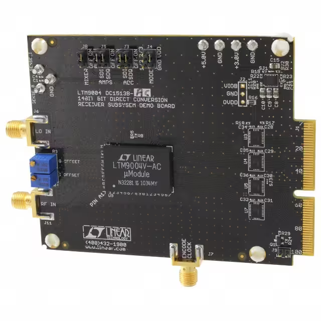
Analog Devices Inc. DC1513B-AC
- Part No.:
- DC1513B-AC
- Manufacturer:
- Analog Devices Inc.
- Category:
- RF, RFID, Wireless Evaluation Boards
- Package:
- Datasheet:
-
 DC1513B-AC.pdf
- Description:
- BOARD EVAL LTM9004-AC
- Quantity:
- Payment:

- Shipping:

Inventory:4,897
Please send an inquiry. Send us your inquiry, and we will respond immediately.
Product details
Overview
DC1513B-AC from Analog Devices (formerly Linear Technology) is a 14-bit direct conversion receiver μModule subsystem integrating dual high-speed ADCs, I/Q demodulator, on-chip broadband transformers, and DC-coupled baseband signal chain. It operates with RF input from 0.7GHz to 2.7GHz, delivers 70.3dB SNR at 9.42MHz baseband bandwidth, and supports 125MHz sampling - deployed in cellular basestation zero-IF receivers requiring high linearity and low DC offset.
For engineers reviewing the DC1513B-AC datasheet, DC1513B-AC pinout, DC1513B-AC application, or DC1513B-AC equivalent, key selection criteria include its 9.42MHz lowpass filter cutoff, 0.2dB I/Q gain mismatch, 1.5° phase mismatch, 3V second-amplifier supply requirement, and 204-lead LGA package thermal performance (θJCbottom = 6.9°C/W).
Technical Context
The DC1513B-AC implements a fully integrated quadrature demodulation architecture with differential gain stages and dual 14-bit ADCs sharing a common RF/LO interface. Its DC-coupled signal path enables precise baseband DC offset adjustment via four dedicated ADJ pins (I±_ADJ, Q±_ADJ), while integrated 50Ω single-ended RF and LO ports eliminate external matching in high-band operation (1.5–2.7GHz).
It features a configurable clock duty cycle stabilizer, optional digital output multiplexer (MUX), and three power management modes (active/sleep/nap). The subsystem uses separate analog supplies: 5V for mixer/first amplifier (VCC1/VCC2), 3V for second amplifier (VCC3), 3V for ADC core (VDD), and 0.5–3.6V for digital outputs (OVDD).
Key Specifications
| Parameter | Value and Actual Design Meaning |
|---|---|
| RF Input Range | 0.7GHz to 2.7GHz - supports cellular bands (700MHz, 1900MHz, 2.1GHz, 2.6GHz) without external matching above 1.5GHz |
| Baseband Bandwidth | DC to 9.42MHz - defines maximum usable IF bandwidth for LTE 20MHz channel reception with guard band |
| ADC Resolution | 14-bit with no missing codes - ensures monotonicity and full-scale dynamic range for high-fidelity I/Q digitization |
| SNR @ 9.42MHz | 70.3dB typical - determines minimum detectable signal level in presence of quantization and thermal noise |
| I/Q Mismatch | 0.2dB gain / 1.5° phase - directly impacts image rejection ratio (typically >45dB) in zero-IF architectures |
| Power Dissipation | 1.83W total - requires thermal design with bottom-side copper and heatsink attachment per θJCbottom = 6.9°C/W |
| Sampling Rate | 125MHz - enables Nyquist-sampled capture of 9.42MHz baseband with oversampling margin |
Pinout & Package
DC1513B-AC is housed in a 204-lead LGA package (15mm × 22mm × 2.91mm) with exposed thermal pad on underside. Pin assignment follows standard LTM9004-AC pinout per Linear Technology documentation (Rev. FA), with GND, VCC1, VCC2, VCC3, VDD, OVDD, OGND, RF, LO, CLKI/CLKQ, I±_ADJ, Q±_ADJ, MIXENABLE, AMP1ENABLE, AMP2ENABLE, ADCSHDNI/Q, OEI/OEQ, MUX, MODE, CLKOUT, OF, DI0–DI13, DQ0–DQ13 distributed across 13×17 grid.
| Pin/Terminal | Circuit Role | Design Meaning |
|---|---|---|
| RF (E2) | Single-ended 50Ω RF input | Accepts 0.7–2.7GHz signal directly; requires series DC-blocking capacitor if source is not AC-coupled |
| LO (H3) | Single-ended 50Ω local oscillator input | Must be DC-blocked externally; internally matched >1.5GHz; shunt cap needed below 1.5GHz |
| I+_ADJ (B1), I–_ADJ (C1) Q+_ADJ (K1), Q–_ADJ (L1) | DC offset trim terminals | Source/sink current to adjust I/Q channel DC offsets independently - critical for zero-IF baseline stability |
| VCC3 (C9, C12, K9, K12) | Second amplifier analog supply | 3V ±0.3V required for LTM9004-AC variant - differs from 5V used in AA/AB versions |
| MUX (D13) | Digital output bus selector | High = Q on DQ[13:0], I on DI[13:0]; Low = swapped; enables shared 14-bit bus for space-constrained PCB layouts |
Key Features
| Feature | Design Value |
|---|---|
| Integrated I/Q demodulator + dual 14-bit ADCs | Eliminates discrete signal chain design effort and layout sensitivity - reduces BOM count by >15 components |
| On-chip 50Ω RF/LO transformers | Removes need for external baluns or matching networks above 1.5GHz - simplifies front-end filtering |
| DC-coupled baseband path with ADJ pins | Enables real-time DC offset correction in closed-loop systems - essential for LTE/LTE-A TDD burst mode |
| Configurable clock duty cycle stabilizer | Maintains <5% jitter degradation across 40–60% input clock duty cycle - improves timing margin in FPGA-driven systems |
| Three power states (Active/Nap/Sleep) | Reduces idle power to 33mW (Nap) or 7mW (Sleep) - extends uptime in battery-backed monitoring applications |
Applications
| Cellular Basestation Receiver | Zero-IF Wireless Infrastructure |
|---|---|
Use Scenario: LTE FDD/TDD macrocell receiver processing 20MHz channels in 1.8–2.2GHz band. IC Role / Device Role / Timing Role: Direct RF-to-baseband conversion subsystem providing synchronized I/Q digitization at 125MSPS. Use Value: 70.3dB SNR and 66dB SFDR enable >30dB carrier-to-interference ratio in dense urban deployments. | Use Scenario: Small-cell remote radio head with embedded digital predistortion (DPD) feedback path. IC Role / Device Role / Timing Role: High-linearity receive path feeding FPGA-based DPD engine with low-latency (<5-cycle) pipeline. Use Value: 0.2dB/1.5° I/Q mismatch ensures >45dB image rejection - critical for accurate DPD coefficient calculation. |
| Software-Defined Radio (SDR) | Test & Measurement Receiver |
Use Scenario: Wideband spectrum analyzer frontend covering 700MHz–2.7GHz with real-time FFT processing. IC Role / Device Role / Timing Role: Digitizes instantaneous baseband after quadrature downconversion - feeds 64k-point FFT engine. Use Value: 9.42MHz lowpass filter cutoff supports 20MHz instantaneous bandwidth with <0.2dB ripple - preserves signal fidelity. | Use Scenario: Benchtop vector signal analyzer requiring calibrated I/Q accuracy and low harmonic distortion. IC Role / Device Role / Timing Role: Reference-grade receive subsystem validating EVM and ACLR of transmitter DUTs. Use Value: 58dB IIP2 and 22dB IIP3 ensure minimal 2nd/3rd-order distortion during multi-tone testing. |
Equivalent & Alternatives
The following parts are listed as comparable options for similar direct conversion receiver applications.
| Alternative Part | Technical Difference | Application Difference | Selection Advice |
|---|---|---|---|
| LTM9004-AC#PBF | Same silicon, identical electrical specs, but offered in tray packaging with Linear/Analog Devices part marking (LTM9004V AC); no evaluation board included | Designed for volume production integration - lacks DC1513B-AC's pre-mounted layout and test points | Select DC1513B-AC for rapid prototyping and lab validation; choose LTM9004-AC#PBF for cost-optimized manufacturing |
| AD9371BBCZ | Higher integration (integrated synthesizer, JESD204B interface, ARM processor); 12-bit dual ADC; 100MHz baseband BW; 8x8 mm CSP vs 22x15 mm LGA | Targets full transceiver systems with digital calibration and embedded firmware - not drop-in compatible | Choose AD9371BBCZ when system-level integration, JESD204B backhaul, or built-in calibration is required |
Compared with LTM9004-AC#PBF, DC1513B-AC provides immediate hardware validation capability; compared with AD9371BBCZ, it offers superior SNR (70.3dB vs 68dB) and lower power (1.83W vs ~3.5W) in simpler zero-IF architectures without synthesizer overhead.
Availability
DC1513B-AC is available at Aetrix Electronics and suitable for cellular basestation development, wireless infrastructure prototyping, and SDR receiver design requiring stable component supply, traceable sourcing, and long-term lifecycle support.
Supply support for DC1513B-AC includes scheduled delivery planning, volume procurement assistance, BOM continuity management, traceable sourcing, and lifecycle availability coordination for OEM customers, industrial embedded developers, connected-device designers, and electronics production programs.
Manufacturer
Analog Devices, Inc. (ADI) is a global leader in high-performance analog, mixed-signal, and digital signal processing technologies, serving communications, industrial, automotive, and healthcare markets.
The DC1513B-AC is part of ADI's μModule receiver product line, designed to simplify high-frequency receiver design by integrating RF, analog, and mixed-signal functions into compact, thermally optimized LGA packages for wireless infrastructure and instrumentation.
FAQ
What is the baseband bandwidth supported by the DC1513B-AC?
The DC1513B-AC supports a baseband frequency range of DC to 9.42MHz, corresponding to its LTM9004-AC variant configuration. This bandwidth is defined by the integrated lowpass filter's 1dB cutoff point and enables full capture of LTE 20MHz channels with guard bands. The value is fixed per device variant and cannot be reconfigured in-circuit.
Does the DC1513B-AC require external RF matching components?
The DC1513B-AC integrates on-chip broadband transformers and requires no external matching network for RF input frequencies between 1.5GHz and 2.7GHz. For operation below 1.5GHz (e.g., 700MHz band), an external series capacitor (and optionally shunt capacitor) is required to transform impedance to 50Ω, as specified in Linear Technology Application Note 9004.
How is DC offset adjusted on the DC1513B-AC?
DC offset is adjusted on the DC1513B-AC using four dedicated pins: I+_ADJ (B1), I–_ADJ (C1), Q+_ADJ (K1), and Q–_ADJ (L1). Current sourced or sunk through these pins trims the DC baseline of each I/Q channel independently. Typical adjustment range is ±35mV with 210µV/°C drift over temperature.
What power supply voltages does the DC1513B-AC require?
The DC1513B-AC requires five distinct supply rails: VCC1/VCC2 = 5V (mixer/first amplifier), VCC3 = 3V (second amplifier, specific to -AC/-AD variants), VDD = 3V (ADC analog core), and OVDD = 0.5–3.6V (digital output drivers). All supplies must be independently bypassed per the LTM9004 layout guidelines.
Can the DC1513B-AC operate in low-power modes?
Yes, the DC1513B-AC supports three power states: Active (1.83W), Nap Mode (33mW), and Sleep Mode (7mW). These are controlled via ADCSHDNI/Q and OEI/OEQ pins. Nap Mode disables ADC clocks while preserving bias; Sleep Mode powers down all analog blocks except reference circuitry.
DC1513B-AC Specifications
- Product attributes
- Attribute value
- Manufacturer:
- Analog Devices Inc.
- Series:
- -
- Packaging:
- Box
- Product Status:
- Active
- Type:
- Direct Conversion Receiver
- Frequency:
- 800MHz ~ 2.7GHz
- Contents:
- Board(s)
- Utilized IC / Part:
- LTM9004
DC1513B-AC FAQ
1.How can I place an order for DC1513B-AC through Aetrix?
Please submit a Request for Quotation (RFQ) for DC1513B-AC on Aetrix. Our sales agent will provide a competitive quotation and guide you through the order confirmation once you accept the terms.
2.Are the price and stock information for DC1513B-AC reliable?
The price and inventory of DC1513B-AC are updated periodically and may fluctuate due to market conditions. Stock and pricing data are typically refreshed every 24 hours. Quotation validity for DC1513B-AC is usually 5 days.
3.What payment methods are accepted for DC1513B-AC?
We accept Wire Transfer, PayPal, Credit Card, Western Union, MoneyGram, and Escrow for DC1513B-AC transactions.
Note: Certain payment methods may incur a processing fee.
4.How is shipping managed for DC1513B-AC?
DC1513B-AC orders can be shipped via leading logistics carriers, including DHL, UPS, FedEx, TNT, or Registered Mail.
Once your DC1513B-AC order is processed, you will receive an email with the shipment details and tracking number.
Note: Tracking information may take up to 24 hours to appear. Express delivery typically takes 3–5 business days.
5.How can I obtain technical support or documentation for DC1513B-AC?
For technical support, including DC1513B-AC datasheets, pinout diagrams, or application guidance, please contact our engineering support team. They can provide detailed documentation and assistance for your DC1513B-AC requirements.
6.How does Aetrix verify that DC1513B-AC is sourced from the original manufacturer or authorized distributors?
All DC1513B-AC products on Aetrix are procured from qualified distributors and authorized channels. Our dedicated quality assurance team conducts strict verification, including traceability checks and, if necessary, third-party testing. This ensures that DC1513B-AC meets industry standards.
7.What is the process for return or replacement of DC1513B-AC?
All DC1513B-AC units undergo pre-shipment inspection (PSI). If there is an issue with DC1513B-AC, returns or replacements are accepted under the following conditions:
1.Quantity discrepancies, incorrect items, or visible external defects (such as breakage or corrosion), acknowledged by Aetrix.
2.The issue is reported within 90 days of delivery.
3.The DC1513B-AC part is unused and in its original packaging.
Return procedure for DC1513B-AC:
1.Submit a request within 90 days.
2.Obtain a Return Material Authorization (RMA) from Aetrix.
DC1513B-AC Tags
-
113991054
Seeed Technology Co., Ltd
-
SC0918
Raspberry Pi

-
113991114
Seeed Technology Co., Ltd
-
ESP32-C6-DEVKITM-1-N4
Espressif Systems
-
ESP32-DEVKITM-1
Espressif Systems
-
C008
M5Stack Technology Co., Ltd.
-
ESP32-C3-DEVKITC-02
Espressif Systems
-
ESP32-C6-DEVKITC-1-N8
Espressif Systems
-
DFR0478
DFRobot
-
102010448
Seeed Technology Co., Ltd
-
ESP32-DEVKITC-32E
Espressif Systems
-
ESP32-DEVKITC-32UE
Espressif Systems
Tech Hub

A practical engineering guide to 3.3V and 5V logic compatibility, input thresholds, resistor dividers, translator ICs, MOSFET level shifting, I2C pull-ups, timing limits and power-sequencing risks.

The 74HC595 uses push-pull logic outputs, while the TPIC6B595 uses 50 V open-drain DMOS sinks for higher-power loads. This guide compares timing, current limits, 3.3 V interfacing, load wiring, thermal…

The 74HC595 converts serial data into eight stable parallel outputs. This guide covers pin functions, shift and storage timing, OE and MR behavior, drive-current limits, cascading, voltage compatibilit…

A technical comparison of level-sensitive latches and edge-triggered flip-flops, covering timing windows, setup and hold limits, master–slave operation, time borrowing, race-through, HDL inference and…

A D latch stores one bit while Enable controls when data can pass. This reference covers gate-level operation, truth tables, transparency, setup and hold timing, LE versus OE, common ICs and practical …

An SR latch stores one bit through cross-coupled feedback. This engineering reference covers NOR and NAND implementations, truth tables, forbidden-state recovery, gated operation, switch debouncing, fa…

Latch circuits retain one bit through feedback. This technical reference covers SR and D latches, truth tables, transparency, timing limits, latch-versus-flip-flop behavior, applications and common log…

An engineering guide to LED driver operation, constant-current and constant-voltage outputs, linear and switching topologies, dimming, IC selection, calculations, replacement compatibility, and fault c…

Operational amplifier guide covering op amp basics, feedback, ideal vs real op amps, common configurations, buffer circuits, offset, bias current, gain-bandwidth, slew rate, rail-to-rail limits and sel…

Jumper cables guide covering safe connection order, red and black clamp placement, final ground connection, cable gauge, length, clamp quality, copper vs CCA cables, jump starter comparison and battery…


