
 My Inquiry
 My Account


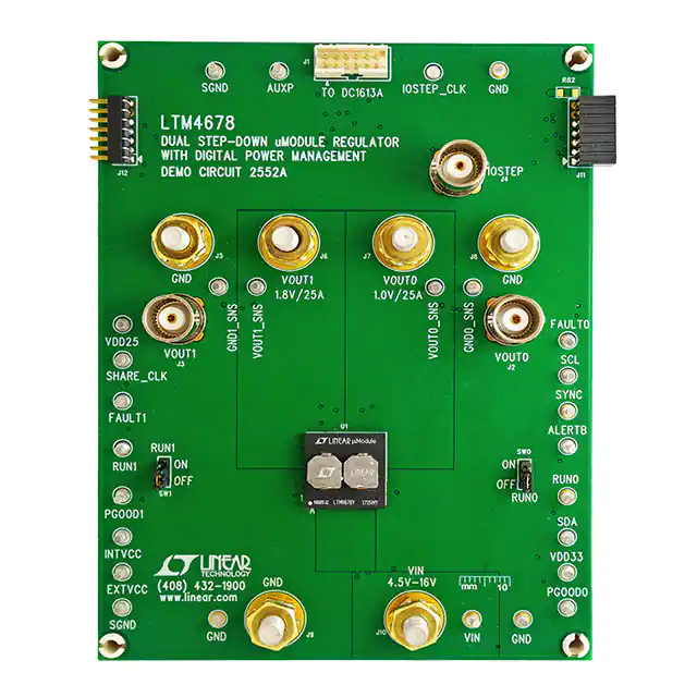
Analog Devices Inc. DC2552A
- Part No.:
- DC2552A
- Manufacturer:
- Analog Devices Inc.
- Package:
- Datasheet:
-
 DC2552A.pdf
- Description:
- EVAL BOARD FOR LTM4678
- Quantity:
- Payment:

- Shipping:

Inventory:4,465
Please send an inquiry. Send us your inquiry, and we will respond immediately.
Product details
Overview
LTM4678 from Analog Devices is a dual 25A or single 50A µModule DC/DC regulator with integrated PMBus digital power system management, featuring dual analog control loops, on-board EEPROM, current-mode PWM, and sub-milliohm DCR current sensing. It delivers tightly regulated 0.5V–3.4V outputs with ±0.5% DC accuracy and supports telemetry polling up to 125Hz in server CPU/GPU core power applications.
For engineers reviewing the LTM4678 datasheet, LTM4678 pinout, LTM4678 application, or LTM4678 equivalent, this page provides verified package mapping (144-pin CoP-BGA), confirmed pin functions (e.g., VOSNS0+/VOSNS0− for differential output voltage sensing), real-world telemetry accuracy specs (±3.5% current readback over –20°C to 125°C), and validated alternatives for high-current digital power delivery systems.
Technical Context
The LTM4678 implements constant-frequency current-mode control per channel with independent programmable soft-start, sequencing delay, and voltage margining via PMBus. Its dual-loop architecture enables simultaneous regulation of two 25A outputs or parallel operation for 50A single-rail delivery.
It integrates a 16-bit ΔΣ ADC, 400kHz PMBus-compliant I²C interface, and on-die temperature sensors with ±1°C internal TUE. Input current sensing uses an integrated amplifier with selectable gain (2×/4×/8×) and ±2% total unadjusted error across its 16mV–64mV full-scale range.
Key Specifications
| Parameter | Value and Actual Design Meaning |
|---|---|
| Output Current | Dual 25A or single 50A continuous - supports high-density CPU/GPU core rail delivery with parallel-phase sharing. |
| Input Voltage Range | 4.5V to 16V - compatible with 5V, 12V intermediate bus architectures without external pre-regulation. |
| Output Voltage Range | 0.5V to 3.4V - digitally adjustable in 244µV LSB steps with ±0.5% DC accuracy over temperature. |
| PMBus Interface | 400kHz I²C-compatible - enables real-time telemetry (voltage, current, temp), fault logging, and configuration via LTpowerPlay GUI. |
| Current Readback Accuracy | ±3.5% over –20°C to 125°C - enables precise load-line calibration and dynamic power budgeting in server platforms. |
| Package | 16mm × 16mm × 5.86mm CoP-BGA (144-pin) - thermally optimized with θJCbottom = 2°C/W for high-power dissipation. |
| Telemetry Polling Rate | Up to 125Hz - supports closed-loop thermal/power management and rapid fault detection in AI accelerators. |
Pinout & Package
144-pin CoP-BGA (16mm × 16mm × 5.86mm) with SnPb or RoHS-compliant terminal finish. Bottom-side thermal pad enhances heat transfer to PCB ground plane.
| Pin/Terminal | Circuit Role | Design Meaning |
|---|---|---|
| VOSNS0+/VOSNS0− | Differential output voltage sense (Channel 0) | Enables Kelvin sensing for ±0.5% regulation accuracy; rejects PCB trace IR drop. |
| VOSNS1+/VOSNS1− | Differential output voltage sense (Channel 1) | Independent sensing path for dual-rail operation; supports asymmetric output configurations. |
| IIN+/IIN− | Differential input current sense inputs | Accepts millivolt-level signals from external shunt; supports ±2% input current telemetry. |
| SHARE_CLK | Phase-interleaving synchronization clock | Enables precise timing alignment between multiple LTM4678s for ripple cancellation and current sharing up to 250A. |
| FAULT0/FAULT1 | Open-drain fault interrupt outputs | Assert low on OV/UV/OT/OC faults; configurable via PMBus to mask non-critical warnings. |
| SDA/SCL | PMBus serial data/clock | 400kHz I²C interface with CRC protection and bus timeout recovery for robust system management. |
Key Features
| Feature | Design Value |
|---|---|
| Dual analog control loops with digital supervision | Combines fast transient response of analog PWM with flexible configuration and telemetry of digital interface - no firmware required for basic operation. |
| Sub-milliohm DCR current sensing | Eliminates external current-sense resistors; reduces BOM cost and board space while maintaining ±3.5% current readback accuracy. |
| Integrated 16-bit ΔΣ ADC | Simultaneously digitizes input/output voltages, currents, temperatures, and uptime with dedicated conversion channels and 90ms default update rate. |
| EEPROM with ECC and fault logging | Stores configuration, calibration data, and runtime fault records (e.g., peak values, uptime, warnings); survives >100k write cycles. |
| Programmable soft-start/ramp rates | Configurable slew rates for VOUT0/VOUT1 enable controlled power-up sequencing in multi-rail SoC systems without external timers. |
Applications
| AI Accelerator Core Power | High-End Server CPU VR |
|---|---|
|
Use Scenario: Supplying dual 25A rails to GPU tensor cores requiring dynamic voltage/frequency scaling under 12.5A/µs load transients. IC Role / Device Role / Timing Role: Dual-channel µModule regulator performing real-time telemetry-driven adaptive voltage positioning (AVP) via PMBus. Use Value: ±50mV peak deviation and 25µs settling time meet PCIe Gen5 GPU power integrity requirements while enabling per-rail power capping. |
Use Scenario: Delivering tightly sequenced 0.8V/1.8V rails to multi-die server CPUs with strict voltage monotonicity and timing windows. IC Role / Device Role / Timing Role: Digitally managed dual-output regulator executing voltage margining, soft-start ramping, and time-based sequencing via pin-strapping or PMBus. Use Value: Programmable TON_DELAYn (down to 0ms) and TON_RISEn (3ms typical) ensure compliance with Intel VRD 14.0 startup timing specifications. |
| Telecom Baseband Unit | Industrial FPGA Power |
|
Use Scenario: Powering 5G massive MIMO RF front-end FPGAs with simultaneous 1.2V core and 1.8V I/O rails under bursty traffic loads. IC Role / Device Role / Timing Role: Dual-output regulator with independent current monitoring per rail and shared thermal telemetry for junction temperature-aware throttling. Use Value: Onboard temperature sensors (±1°C TUE) and 125Hz telemetry polling enable predictive thermal derating before FPGA thermal shutdown. |
Use Scenario: Providing reconfigurable 0.75V–3.3V supplies to Xilinx Versal ACAPs in harsh industrial environments with wide ambient temperature swings. IC Role / Device Role / Timing Role: Robust µModule with –40°C to 125°C operating range, undervoltage lockout (UVLO) at 3.55V, and fault-logging EEPROM for field diagnostics. Use Value: ±0.5% DC output accuracy and ±3.5% current readback over full temperature range eliminate need for external calibration in mission-critical PLC designs. |
Equivalent & Alternatives
The following parts are listed as comparable options for similar high-current digital power delivery applications.
| Alternative Part | Technical Difference | Application Difference | Selection Advice |
|---|---|---|---|
| LTM4677 | Single 50A output only; lacks dual-channel independence and separate VOSNSx pairs. | Suitable for single-rail systems but cannot support asymmetric dual-rail sequencing or independent telemetry per rail. | Select LTM4677 only when board space is constrained and dual-rail isolation is unnecessary. |
| TPS546D24A | 60A single-channel buck with PMBus; no integrated inductors or CoP-BGA package - requires external magnetics and layout optimization. | Offers higher peak current but demands significant PCB area and thermal design effort versus LTM4678's drop-in module form factor. | Choose TPS546D24A when maximum flexibility in inductor selection and custom loop compensation is required. |
Compared with LTM4678, LTM4677 sacrifices dual-rail telemetry and independent control for smaller footprint, while TPS546D24A trades integration and thermal performance for higher current scalability and design flexibility - making LTM4678 optimal for space-constrained, thermally demanding dual-rail applications requiring out-of-box telemetry.
Availability
LTM4678 is available at Aetrix Electronics and suitable for AI accelerator core power, high-end server CPU VR, telecom baseband unit, and industrial FPGA power applications requiring stable component supply, long-term lifecycle support, and traceable sourcing.
Supply support for LTM4678 includes scheduled delivery planning, volume procurement assistance, BOM continuity management, traceable sourcing, and lifecycle availability coordination for OEM customers, industrial embedded developers, connected-device designers, and electronics production programs.
Manufacturer
Analog Devices is a global leader in high-performance analog, mixed-signal, and digital signal processing semiconductors, serving precision instrumentation, communications, and power management markets.
The LTM4678 belongs to the µModule regulator product line, designed specifically for high-current, digitally managed power delivery in space-constrained computing and infrastructure systems where integration, telemetry, and reliability are critical.
FAQ
What is the maximum supported PMBus telemetry polling rate for the LTM4678?
The LTM4678 supports telemetry polling up to 125Hz via its 400kHz PMBus interface. This rate is achievable using the MFR_ADC_CONTROL register to configure faster ADC conversion modes. At default settings, the update interval is 90ms, but selecting specific ADC channels (e.g., MFR_ADC_CONTROL = 0x06 for Channel 0 current) reduces it to 8ms. The LTM4678 maintains full telemetry fidelity-including voltage, current, temperature, and uptime-across all supported polling rates without sacrificing accuracy.
Does the LTM4678 require external current-sense resistors for output current monitoring?
No, the LTM4678 does not require external current-sense resistors for output current monitoring. It implements sub-milliohm DCR current sensing using the inductor's inherent DC resistance, eliminating the need for discrete shunts. This approach reduces power loss, board area, and BOM cost while maintaining ±3.5% current readback accuracy over –20°C to 125°C. The LTM4678 also integrates an input current sense amplifier with selectable gain for accurate input telemetry without external components.
Can the LTM4678 operate as a single 50A regulator, and how is phase interleaving configured?
Yes, the LTM4678 can operate as a single 50A regulator by paralleling both channels. Phase interleaving is configured via the FSWPH_CFG pin-strapping resistor network or through the PMBus MFR_PHASE command. When set to 180° interleaving, the LTM4678 reduces input/output ripple amplitude and improves thermal distribution across the module. The SHARE_CLK pin synchronizes switching edges between multiple LTM4678 units, enabling scalable current sharing up to 250A in multi-module configurations.
What is the purpose of the VOSNS0+/VOSNS0− and VOSNS1+/VOSNS1− pins on the LTM4678?
The VOSNS0+/VOSNS0− and VOSNS1+/VOSNS1− pins provide Kelvin (4-wire) differential sensing for Channel 0 and Channel 1 output voltages, respectively. This topology rejects voltage drops across PCB traces and connectors, enabling the LTM4678 to maintain ±0.5% DC output regulation accuracy over line, load, and temperature. Each pair connects directly to the load point, allowing precise closed-loop control independent of routing losses - a critical capability for low-voltage, high-current applications like CPU core rails.
How does the LTM4678 handle fault conditions such as overvoltage or overtemperature?
The LTM4678 detects overvoltage (OV), undervoltage (UV), overtemperature (OT), and overcurrent (OC) faults using dedicated analog comparators and digital thresholds programmed via PMBus. Upon fault detection, it asserts the corresponding FAULT0 or FAULT1 pin, logs the event in onboard EEPROM with timestamp and peak values, and executes configurable responses - including immediate shutdown, latched-off state, or warning-only reporting. The LTM4678 supports masking non-critical faults via ALERT register configuration to prevent false system resets during transient events.
DC2552A Specifications
- Product attributes
- Attribute value
- Manufacturer:
- Analog Devices Inc.
- Series:
- µModule®
- Packaging:
- Box
- Product Status:
- Active
- Main Purpose:
- DC/DC, Step Down
- Outputs and Type:
- 2 Non-Isolated Outputs
- Voltage - Output:
- -
- Current - Output:
- 1V, 1.8V
- Voltage - Input:
- 25A, 25A
- Regulator Topology:
- 4.5V ~ 16V
- Frequency - Switching:
- Buck
- Contents:
- 500kHz
- Utilized IC / Part:
- Board(s)
- Power - Output:
- LTM4678
DC2552A FAQ
1.How can I place an order for DC2552A through Aetrix?
Please submit a Request for Quotation (RFQ) for DC2552A on Aetrix. Our sales agent will provide a competitive quotation and guide you through the order confirmation once you accept the terms.
2.Are the price and stock information for DC2552A reliable?
The price and inventory of DC2552A are updated periodically and may fluctuate due to market conditions. Stock and pricing data are typically refreshed every 24 hours. Quotation validity for DC2552A is usually 5 days.
3.What payment methods are accepted for DC2552A?
We accept Wire Transfer, PayPal, Credit Card, Western Union, MoneyGram, and Escrow for DC2552A transactions.
Note: Certain payment methods may incur a processing fee.
4.How is shipping managed for DC2552A?
DC2552A orders can be shipped via leading logistics carriers, including DHL, UPS, FedEx, TNT, or Registered Mail.
Once your DC2552A order is processed, you will receive an email with the shipment details and tracking number.
Note: Tracking information may take up to 24 hours to appear. Express delivery typically takes 3–5 business days.
5.How can I obtain technical support or documentation for DC2552A?
For technical support, including DC2552A datasheets, pinout diagrams, or application guidance, please contact our engineering support team. They can provide detailed documentation and assistance for your DC2552A requirements.
6.How does Aetrix verify that DC2552A is sourced from the original manufacturer or authorized distributors?
All DC2552A products on Aetrix are procured from qualified distributors and authorized channels. Our dedicated quality assurance team conducts strict verification, including traceability checks and, if necessary, third-party testing. This ensures that DC2552A meets industry standards.
7.What is the process for return or replacement of DC2552A?
All DC2552A units undergo pre-shipment inspection (PSI). If there is an issue with DC2552A, returns or replacements are accepted under the following conditions:
1.Quantity discrepancies, incorrect items, or visible external defects (such as breakage or corrosion), acknowledged by Aetrix.
2.The issue is reported within 90 days of delivery.
3.The DC2552A part is unused and in its original packaging.
Return procedure for DC2552A:
1.Submit a request within 90 days.
2.Obtain a Return Material Authorization (RMA) from Aetrix.
DC2552A Tags
-
DFR0571
DFRobot
-
DFR0379
DFRobot
-
DFR0205
DFRobot
-
1385
Adafruit Industries LLC
-
COM-15208
SparkFun Electronics
-
1944
Adafruit Industries LLC
-
2465
Adafruit Industries LLC
-
DC2468A
Analog Devices Inc.
-
DC2841A
Analog Devices Inc.

-
TPS552892EVM-111
Texas Instruments
-
TPS55289EVM-093
Texas Instruments
-
EPC9158
EPC
Tech Hub

A practical engineering guide to 3.3V and 5V logic compatibility, input thresholds, resistor dividers, translator ICs, MOSFET level shifting, I2C pull-ups, timing limits and power-sequencing risks.

The 74HC595 uses push-pull logic outputs, while the TPIC6B595 uses 50 V open-drain DMOS sinks for higher-power loads. This guide compares timing, current limits, 3.3 V interfacing, load wiring, thermal…

The 74HC595 converts serial data into eight stable parallel outputs. This guide covers pin functions, shift and storage timing, OE and MR behavior, drive-current limits, cascading, voltage compatibilit…

A technical comparison of level-sensitive latches and edge-triggered flip-flops, covering timing windows, setup and hold limits, master–slave operation, time borrowing, race-through, HDL inference and…

A D latch stores one bit while Enable controls when data can pass. This reference covers gate-level operation, truth tables, transparency, setup and hold timing, LE versus OE, common ICs and practical …

An SR latch stores one bit through cross-coupled feedback. This engineering reference covers NOR and NAND implementations, truth tables, forbidden-state recovery, gated operation, switch debouncing, fa…

Latch circuits retain one bit through feedback. This technical reference covers SR and D latches, truth tables, transparency, timing limits, latch-versus-flip-flop behavior, applications and common log…

An engineering guide to LED driver operation, constant-current and constant-voltage outputs, linear and switching topologies, dimming, IC selection, calculations, replacement compatibility, and fault c…

Operational amplifier guide covering op amp basics, feedback, ideal vs real op amps, common configurations, buffer circuits, offset, bias current, gain-bandwidth, slew rate, rail-to-rail limits and sel…

Jumper cables guide covering safe connection order, red and black clamp placement, final ground connection, cable gauge, length, clamp quality, copper vs CCA cables, jump starter comparison and battery…


