
 My Inquiry
 My Account


STMicroelectronics DEMOTD350
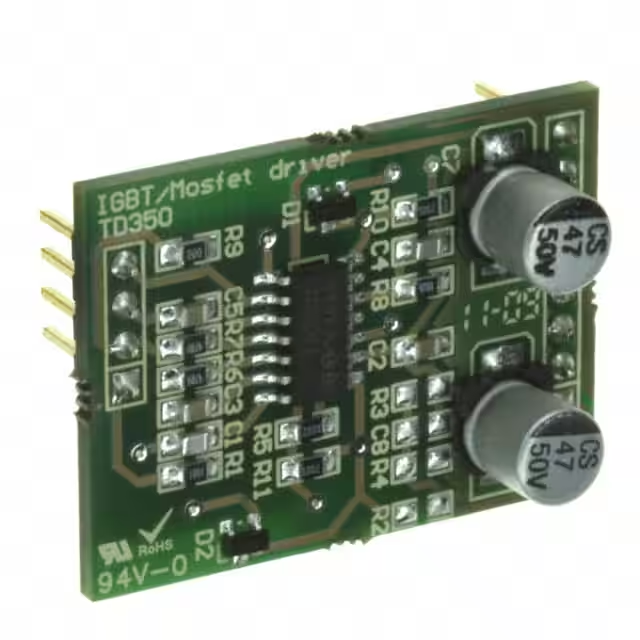
- Part No.:
- DEMOTD350
- Manufacturer:
- STMicroelectronics
- Package:
- Datasheet:
-
 DEMOTD350.pdf
- Description:
- EVAL BOARD FOR TD350
- Quantity:
- Payment:

- Shipping:

Inventory:3,976
Please send an inquiry. Send us your inquiry, and we will respond immediately.
Product details
Overview
TD350 from STMicroelectronics is an advanced IGBT and power MOSFET gate driver IC featuring 1.5 A source / 2.3 A sink typical gate drive capability, active Miller clamp, two-step turn-off with adjustable level and delay, desaturation detection, and fault status output. It operates across -40°C to +125°C, supports ±10 V gate drive (VH = 16 V, VL = -10 V), and is used in 1200 V three-phase inverters for motor control and UPS systems.
For engineers reviewing the TD350 datasheet, TD350 pinout, TD350 application, or TD350 equivalent, key selection considerations include its dual-sink/source outputs for independent gate control, programmable two-level turn-off timing, integrated desat protection with 7.2 V threshold, and compatibility with optocouplers or pulse transformers in high-reliability industrial power stages.
Technical Context
The TD350 implements a dedicated analog control block with separate high-side (OUTH) and low-side (OUTL) gate drive outputs, enabling precise charge/discharge path separation without external diodes. Its active Miller clamp activates at 2.0 V gate voltage (relative to GND) and clamps to VL+3.0 V max under 500 mA Miller current.
Two-level turn-off uses external COFF capacitor and LVOFF voltage to set delay (Ta) and off-level; same delay applies at turn-on to prevent pulse width distortion. Desaturation detection triggers at 7.2 V on DESAT pin with internal blanking via 250 µA current source and external capacitor.
Key Specifications
| Parameter | Value and Actual Design Meaning |
|---|---|
| Gate Drive Strength | 1.5 A source / 2.3 A sink typical at 25°C; enables fast switching of high-Ciss IGBTs up to 1200 V class |
| Desat Threshold | 7.2 V typ; detects IGBT saturation loss during overcurrent/short-circuit with 500 ns fault response |
| Miller Clamp Threshold | 2.0 V; activates clamp output (CLAMP pin) to suppress false turn-on during high dV/dt commutation |
| UVLO Threshold | 10 V (top), 10 V (bottom) with 1 V hysteresis; disables OUTH and pulls OUTL low below safe supply level |
| Propagation Delay | 400–650 ns turn-on, 300–620 ns turn-off; ensures tight timing control in high-frequency inverter PWM |
| ESD Rating | 2 kV HBM; provides robust handling during PCB assembly and system integration |
| Supply Range | VH = UVLO to 26 V, VL = 0 to –10 V; supports bootstrap high-side and isolated negative bias configurations |
Pinout & Package
TD350 is housed in a SO-14 surface-mount package with standard 1.27 mm pitch, ECOPACK®-compliant lead-free finish, and thermal resistance RthJA = 125 °C/W.
| Pin/Terminal | Circuit Role | Design Meaning |
|---|---|---|
| IN | Input trigger | Active-low logic input compatible with optocoupler or pulse transformer; edge-triggered with 100 ns minimum pulse width |
| VREF | Voltage reference output | +5.0 V ±2% reference for accurate timing of two-level turn-off using external RC network |
| FAULT | Fault status output | Open-drain digital output signaling desat or UVLO; designed to directly drive optocoupler LED |
| NC | No connect | Pin 4 and Pin 6 are internally unconnected; must be left floating or grounded per layout best practice |
| COFF | Turn-off delay timing | Capacitor connection point setting two-level turn-off delay (Ta); internal 500 Ω discharge resistor |
| LVOFF | Turn-off level control | Analog input setting second-stage gate voltage level during two-step turn-off; 120–200 µA sink current |
| GND | Signal ground | Reference node for IN, FAULT, DESAT, CLAMP, and VREF; requires low-impedance PCB return path |
| CLAMP | Miller clamp output | Active-low clamp driver activated when gate voltage falls below 2.0 V; sinks up to 500 mA |
| VL | Negative supply | –10 V rail for negative gate bias; enables reliable IGBT turn-off and noise immunity |
| OUTL | Gate sink output | Low-side gate driver output; delivers 2.3 A sink current for rapid IGBT/MOSFET discharge |
| OUTH | Gate source output | High-side gate driver output; sources 1.5 A to charge gate capacitance quickly |
| VH | Positive supply | +16 V nominal positive rail; powers OUTH and internal logic; UVLO triggers below 10 V |
| DESAT | Desaturation sense input | Analog input monitoring IGBT collector-emitter voltage via RC snubber; trips at 7.2 V threshold |
Key Features
| Feature | Design Value |
|---|---|
| Separate sink/source outputs | Enables independent optimization of gate charge (OUTH) and discharge (OUTL) paths without external diodes or resistors |
| Active Miller clamp | Eliminates need for negative gate supply in most applications by clamping gate to VL+3.0 V during high dV/dt |
| Two-step turn-off | Programmable delay (Ta) and off-level reduce IGBT overvoltage and RBSOA stress during short-circuit events |
| Integrated desat detection | 7.2 V threshold with internal blanking time prevents false triggering during normal IGBT saturation |
| Optocoupler/pulse transformer input | Active-low input interface simplifies isolation design and reduces component count in high-voltage gate drive stages |
Applications
| Industrial Motor Drives | Uninterruptible Power Supplies (UPS) |
|---|---|
|
Use Scenario: Three-phase 1200 V IGBT inverter driving induction motors in HVAC compressors and industrial pumps. IC Role / Device Role / Timing Role: High-reliability gate driver providing active Miller clamp, two-step turn-off, and desat protection during overload transients. Use Value: Prevents destructive shoot-through and overvoltage failure during rapid load changes, extending IGBT lifetime in continuous-duty cycles. |
Use Scenario: Online double-conversion UPS with bidirectional IGBT bridges for battery charging and AC output inversion. IC Role / Device Role / Timing Role: Fault-tolerant gate driver delivering synchronized high-side/low-side control with real-time desat monitoring. Use Value: Enables immediate shutdown on IGBT desaturation, avoiding DC bus collapse and ensuring clean transfer to battery backup mode. |
| Solar Inverters | Industrial Welding Equipment |
|
Use Scenario: String inverters using 1200 V IGBT modules in MPPT and grid-synchronization stages. IC Role / Device Role / Timing Role: Precision gate driver supporting high-frequency PWM with <650 ns propagation delay and <50 ns pulse distortion. Use Value: Maintains tight dead-time control and minimizes conduction losses while ensuring safe commutation under variable irradiance. |
Use Scenario: IGBT-based inverter welders requiring robust short-circuit protection during arc initiation and metal transfer. IC Role / Device Role / Timing Role: Fast-fault gate driver with 500 ns desat response and programmable two-level turn-off to limit peak short-circuit current. Use Value: Reduces IGBT junction temperature rise during repeated short-circuits, preventing thermal runaway in high-duty-cycle welding cycles. |
Equivalent & Alternatives
The following parts are listed as comparable options for similar IGBT gate driver applications.
| Alternative Part | Technical Difference | Application Difference | Selection Advice |
|---|---|---|---|
| IR2110S | Lower drive strength (2 A sink/2 A source), no active Miller clamp, no two-step turn-off, no integrated desat detection | Requires external desat circuit and negative bias for Miller immunity; suited for lower-power or cost-sensitive designs | Select when system-level protection is implemented externally and gate drive requirements are ≤600 V IGBTs |
| UCC27324 | Single-channel, 4 A sink/4 A source, no desat/UVLO/fault reporting, no Miller clamp, no two-step turn-off | Designed for discrete MOSFETs only; lacks IGBT-specific protection and high-voltage isolation interface | Select only for low-side, non-isolated, high-speed MOSFET gate driving where full protection is handled upstream |
Compared with IR2110S and UCC27324, TD350 uniquely integrates desat detection, active Miller clamp, and two-step turn-off in a single SO-14 package-enabling compact, high-reliability 1200 V IGBT control without external protection components or negative bias supplies.
Availability
TD350 is available at Aetrix Electronics and suitable for industrial motor drives, uninterruptible power supplies (UPS), solar inverters, and industrial welding equipment requiring stable component supply and long-term lifecycle support.
Supply support for TD350 includes scheduled delivery planning, volume procurement assistance, BOM continuity management, traceable sourcing, and lifecycle availability coordination for OEM customers, industrial embedded developers, connected-device designers, and electronics production programs.
Manufacturer
STMicroelectronics is a global semiconductor leader headquartered in Geneva, Switzerland, designing and manufacturing microcontrollers, power ICs, sensors, and automotive-grade components.
TD350 belongs to ST's high-voltage gate driver product line, engineered specifically for robust IGBT and MOSFET control in industrial inverters, UPS, and motor drives demanding integrated protection and high-temperature operation.
FAQ
What is the purpose of the CLAMP pin on TD350?
The CLAMP pin provides active Miller current control during high dV/dt switching events. When the gate voltage drops below 2.0 V relative to GND, CLAMP activates and sinks up to 500 mA to hold the gate near VL+3.0 V, preventing false turn-on without requiring a negative supply rail. This function is automatically disabled upon next IN signal activation.
How does the two-step turn-off feature protect the IGBT?
During overcurrent or short-circuit, the two-step turn-off first reduces gate voltage to a user-defined level (via LVOFF) after a programmable delay (set by COFF), limiting di/dt and collector voltage rise. Then it fully turns off the device, reducing both overvoltage stress and RBSOA violation risk. The same delay applies at turn-on to avoid pulse width distortion.
Can TD350 drive both IGBTs and MOSFETs?
Yes-TD350 is explicitly qualified for both IGBTs and power MOSFETs. Its 1.5 A source / 2.3 A sink drive strength, ±10 V gate swing capability (VH=16 V, VL=–10 V), and desaturation detection (optimized for IGBT VCE) make it suitable for high-voltage IGBTs, while its fast propagation delays (<650 ns) and Miller clamp also benefit high-speed Si/SiC MOSFETs in hard-switched topologies.
Is TD350 still in active production?
TD350 is marked "Obsolete Product(s)" in its official STMicroelectronics documentation (Doc ID 9525 Rev 6, April 2010). However, Aetrix Electronics maintains legacy inventory and offers extended supply support-including traceable lots, engineering documentation, and lifecycle coordination-for industrial customers continuing to use this mature, field-proven gate driver in existing designs.
DEMOTD350 Specifications
- Product attributes
- Attribute value
- Manufacturer:
- STMicroelectronics
- Series:
- -
- Packaging:
- Bulk
- Product Status:
- Active
- Type:
- Power Management
- Function:
- FET Driver (External FET)
- Embedded:
- No
- Utilized IC / Part:
- TD350
- Primary Attributes:
- 750mA Source/1.2A Sink, Active Miller Clamp
- Secondary Attributes:
- Negative Gate Drive Ability, Fault Status Output, UVLO and ESD Protection
- Contents:
- Board(s)
DEMOTD350 FAQ
1.How can I place an order for DEMOTD350 through Aetrix?
Please submit a Request for Quotation (RFQ) for DEMOTD350 on Aetrix. Our sales agent will provide a competitive quotation and guide you through the order confirmation once you accept the terms.
2.Are the price and stock information for DEMOTD350 reliable?
The price and inventory of DEMOTD350 are updated periodically and may fluctuate due to market conditions. Stock and pricing data are typically refreshed every 24 hours. Quotation validity for DEMOTD350 is usually 5 days.
3.What payment methods are accepted for DEMOTD350?
We accept Wire Transfer, PayPal, Credit Card, Western Union, MoneyGram, and Escrow for DEMOTD350 transactions.
Note: Certain payment methods may incur a processing fee.
4.How is shipping managed for DEMOTD350?
DEMOTD350 orders can be shipped via leading logistics carriers, including DHL, UPS, FedEx, TNT, or Registered Mail.
Once your DEMOTD350 order is processed, you will receive an email with the shipment details and tracking number.
Note: Tracking information may take up to 24 hours to appear. Express delivery typically takes 3–5 business days.
5.How can I obtain technical support or documentation for DEMOTD350?
For technical support, including DEMOTD350 datasheets, pinout diagrams, or application guidance, please contact our engineering support team. They can provide detailed documentation and assistance for your DEMOTD350 requirements.
6.How does Aetrix verify that DEMOTD350 is sourced from the original manufacturer or authorized distributors?
All DEMOTD350 products on Aetrix are procured from qualified distributors and authorized channels. Our dedicated quality assurance team conducts strict verification, including traceability checks and, if necessary, third-party testing. This ensures that DEMOTD350 meets industry standards.
7.What is the process for return or replacement of DEMOTD350?
All DEMOTD350 units undergo pre-shipment inspection (PSI). If there is an issue with DEMOTD350, returns or replacements are accepted under the following conditions:
1.Quantity discrepancies, incorrect items, or visible external defects (such as breakage or corrosion), acknowledged by Aetrix.
2.The issue is reported within 90 days of delivery.
3.The DEMOTD350 part is unused and in its original packaging.
Return procedure for DEMOTD350:
1.Submit a request within 90 days.
2.Obtain a Return Material Authorization (RMA) from Aetrix.
DEMOTD350 Tags
-
BOB-12009
SparkFun Electronics
-
106990290
Seeed Technology Co., Ltd
-
BOB-11771
SparkFun Electronics
-
BOB-09118
SparkFun Electronics

-
4410
Adafruit Industries LLC
-
5335
Adafruit Industries LLC
-
BOB-11189
SparkFun Electronics
-
3295
Adafruit Industries LLC
-
3421
Adafruit Industries LLC
-
1904
Adafruit Industries LLC
-
2717
Adafruit Industries LLC
-
3190
Adafruit Industries LLC
Tech Hub

An engineering guide to LED driver operation, constant-current and constant-voltage outputs, linear and switching topologies, dimming, IC selection, calculations, replacement compatibility, and fault c…

Operational amplifier guide covering op amp basics, feedback, ideal vs real op amps, common configurations, buffer circuits, offset, bias current, gain-bandwidth, slew rate, rail-to-rail limits and sel…

Jumper cables guide covering safe connection order, red and black clamp placement, final ground connection, cable gauge, length, clamp quality, copper vs CCA cables, jump starter comparison and battery…

LDO regulator guide covering low dropout voltage, power dissipation, thermal design, PSRR, output noise, capacitor stability, adjustable LDO circuits, LDO vs buck converter and datasheet selection chec…

Conditional Access Module guide covering CAM meaning, CI/CI+ interface, smart card authorization, DVB security workflow, TV and set-top box compatibility, internal electronics, ESD protection, connecto…

Guide to electronic component obsolescence covering EOL risk, PCN/PDN notices, last-time buy planning, replacement options, form-fit-function validation, counterfeit risk and BOM lifecycle management.

18650 battery guide covering lithium-ion cell basics, 3.6V/3.7V voltage, 4.2V charging, mAh and Wh capacity, protected cells, chargers, BMS, series-parallel packs, holders, welding and sourcing checks.…

Hall effect sensor guide covering working principle, linear and digital sensors, Arduino circuits, current sensing, speed detection, automotive applications, A3144 examples, signal filtering and datash…

Product Change Notification guide for electronic components, covering PCN meaning, PCN vs PDN/EOL, common change types, risk levels, form-fit-function review, engineering validation, BOM control, LTB/L…

A practical guide to blend door actuators, covering HVAC function, symptoms, location, AC and heater issues, reset and calibration, replacement cost, electrical diagnosis, compatibility checks, and rep…


