
 My Inquiry
 My Account


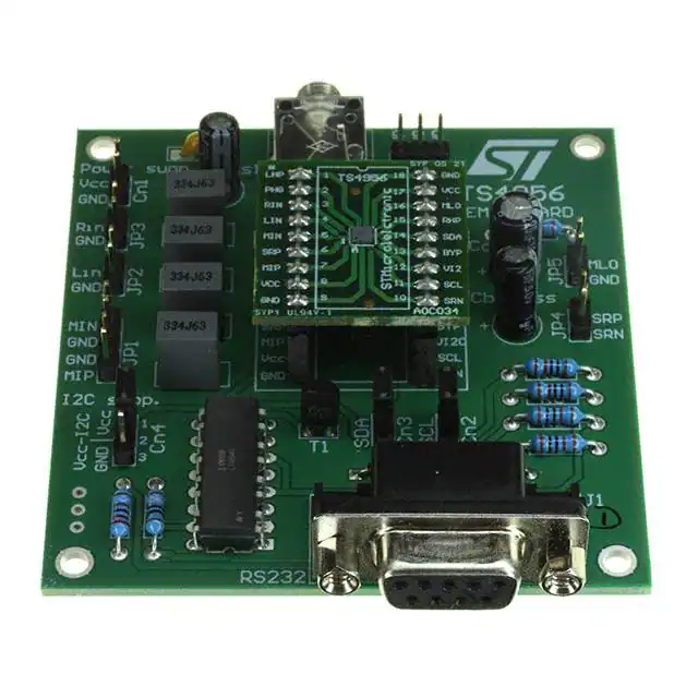
STMicroelectronics DEMOTS4956J
- Part No.:
- DEMOTS4956J
- Manufacturer:
- STMicroelectronics
- Category:
- Audio Amplifier Evaluation Boards
- Package:
- Datasheet:
-
 DEMOTS4956J.pdf
- Description:
- EVAL BOARD FOR TS4956
- Quantity:
- Payment:

- Shipping:

Inventory:2,314
Please send an inquiry. Send us your inquiry, and we will respond immediately.
Product details
Overview
TS4956 from STMicroelectronics is a stereo audio amplifier system with integrated I²C bus interface, delivering 38 mW per channel into 16 Ω at 3.3 V (1% THD+N), supporting 8 output modes including BTL speaker drive and phantom-ground headphone output, and featuring ultra-low 0.5 µA standby current for mobile audio subsystems.
For engineers reviewing the TS4956 datasheet, TS4956 pinout, TS4956 application, or TS4956 equivalent, this device enables flexible audio routing in space-constrained portable designs requiring digital volume control (−34.5 dB to +12 dB in 1.5 dB steps), pop/click suppression, thermal shutdown protection, and I²C-configurable gain/output mode selection without external passive components.
Technical Context
The TS4956 integrates three independent output stages-stereo headphone (LHP+/LHP−), mono loudspeaker (SRP+/SRN−), and mono line-out (MLO)-each selectable via I²C register bits D2–D0. Its digital gain control operates across −34.5 dB to +12 dB in precise 1.5 dB steps, with step error ≤0.6 dB, and supports differential (MIP/MIN) or single-ended (LIN/RIN) input configurations depending on selected mode.
It implements flip-chip packaging with 18 bumps (300 µm diameter), thermal shutdown activation at 150 °C, and PSRR up to 77 dB (mode 4, 217 Hz). The I²C interface operates at up to 400 kHz with dedicated I2CVCC supply pin enabling independent logic-level control and nanoamp-level total standby when grounded.
Key Specifications
| Parameter | Value and Actual Design Meaning |
|---|---|
| Supply Voltage | 2.7 V to 5.5 V - supports direct connection to Li-ion battery or regulated 3.3 V/5 V rails without LDO. |
| Headphone Output Power | 32 mW per channel @ 3.3 V, 16 Ω, 1% THD+N - sufficient for high-sensitivity earpieces without clipping. |
| BTL Speaker Output Power | 450 mW @ 3.3 V, 8 Ω, 1% THD+N - drives small speakers in mobile handsets or wearables. |
| Digital Volume Range | −34.5 dB to +12 dB in 1.5 dB steps - enables fine-grained loudness matching across diverse transducers. |
| Standby Current | 0.5 µA - extends battery life during audio idle periods in always-on voice interfaces. |
| I²C Clock Frequency | Up to 400 kHz - compatible with standard fast-mode I²C controllers without timing margin concerns. |
| THD+N | ≤0.5% @ 20 Hz–20 kHz - ensures clean playback across audible spectrum with minimal harmonic distortion. |
| PSRR | 77 dB (mode 4) - rejects power rail noise from noisy DC-DC converters in mixed-signal SoC platforms. |
Pinout & Package
TS4956 uses a lead-free flip-chip package with 18 bumps (300 µm diameter), optimized for compact PCB layout and thermal performance (RthJA = 90 °C/W with 120 mm² heat sink surface).
| Pin/Terminal | Circuit Role | Design Meaning |
|---|---|---|
| RIN | Stereo right input (single-ended) | Accepts analog audio signal referenced to ground; used in modes 2, 4, 6, 7. |
| LIN | Stereo left input (single-ended) | Accepts analog audio signal referenced to ground; used in modes 2, 4, 6, 7. |
| MIP / MIN | Mono differential input pair | Enables noise-rejecting input configuration for hands-free microphone or auxiliary sources (modes 1, 3, 5). |
| RHP+ / RHP− | Right headphone output (phantom-ground) | Delivers balanced drive to stereo headphones; eliminates DC-blocking capacitors in AC-coupled paths. |
| SRP+ / SRN− | Speaker BTL output pair | Provides bridge-tied load drive for 8 Ω speakers with doubled voltage swing and higher efficiency. |
| MLO | Mono line-out output | Single-ended buffered output for hands-free speakerphone or auxiliary line-level connection (modes 5, 6). |
| SDA / SCL | I²C data and clock | Open-drain bidirectional interface; requires external 10 kΩ pull-ups for MCU communication. |
| I2CVCC | I²C logic supply | Independent voltage domain for I²C interface; grounding disables I²C and forces ultra-low standby. |
| BYPASS | Half-supply reference bypass | Connects to 1 µF capacitor to stabilize internal virtual ground for phantom-ground headphone operation. |
| VCC / GND | Main power and ground | Dual VCC pins reduce IR drop; GND pins provide low-impedance return paths for analog and digital sections. |
Key Features
| Feature | Design Value |
|---|---|
| 8 configurable output modes | Selectable via I²C D2–D0 bits - enables single design to serve headphone, speaker, hands-free, and BTL applications. |
| Pop and click reduction circuitry | Hardware-based soft-start and mute sequencing - eliminates audible transients during power-up/down and mode switching. |
| Internal thermal shutdown | Activates at 150 °C junction temperature - protects device and PCB during sustained high-power operation or poor heatsinking. |
| Digital volume control | 32-step, ±0.6 dB step accuracy - avoids analog potentiometer drift and enables firmware-controlled loudness calibration. |
| Ultra-low standby current | 0.5 µA with I2CVCC grounded - reduces system quiescent draw below typical RTC or sensor node requirements. |
| Flip-chip 18-bump package | 300 µm bump pitch, no wire bonds - improves RF immunity, thermal conduction, and board-level reliability in handheld assemblies. |
Applications
| Mobile Handset Audio Subsystem | Portable Media Player Headphone Drive |
|---|---|
|
Use Scenario: Integrated audio solution in GSM/UMTS smartphones handling simultaneous headset, speakerphone, and loudspeaker playback. IC Role / Device Role / Timing Role: Central audio hub managing I²C-configured routing between baseband processor, stereo DAC outputs, and three physical outputs. Use Value: Eliminates 12+ discrete components (capacitors, resistors, op-amps) while enabling dynamic reconfiguration of output topology during call vs. media playback. |
Use Scenario: High-fidelity headphone output in MP3 players with battery life optimization and zero-pop user experience. IC Role / Device Role / Timing Role: Phantom-ground headphone driver with digital volume control and integrated pop suppression logic. Use Value: Delivers 32 mW/channel into 16 Ω without DC-blocking caps, reducing BOM cost and PCB area by >30% versus discrete Class AB solutions. |
| Tablet Hands-Free Speakerphone | Wearable Voice Assistant Output |
|
Use Scenario: Dual-mic voice capture and loudspeaker playback in Android tablets with echo cancellation support. IC Role / Device Role / Timing Role: Mono line-out (MLO) for analog mic preamp feedback path and BTL speaker drive (mode 7) for near-field audio output. Use Value: Enables full-duplex operation using shared I²C bus for gain synchronization between mic input and speaker output paths. |
Use Scenario: Compact voice prompt delivery in Bluetooth earbuds or smartwatches with strict size and power constraints. IC Role / Device Role / Timing Role: Low-quiescent-current headphone driver (mode 3/4) with wake-up time <90 ms for responsive voice feedback. Use Value: Achieves 120-hour standby on 100 mAh battery due to 0.5 µA shutdown current, exceeding typical wearable runtime targets. |
Equivalent & Alternatives
The following parts are listed as comparable options for similar stereo audio amplifier with I²C control applications.
| Alternative Part | Technical Difference | Application Difference | Selection Advice |
|---|---|---|---|
| MAX98357A | Class D, I²S input only, no analog inputs or headphone drive - requires external DAC and lacks MLO/SRP+ outputs. | Targeted at speaker-only systems; cannot replace TS4956's integrated headphone + speaker + line-out triple-output capability. | Select only if system already includes high-quality stereo DAC and requires >85% efficiency at >100 mW output. |
| TAS5707 | Class D, 4-channel, I²S/PDM input, no analog inputs - supports BTL but no phantom-ground headphone mode or MLO output. | Designed for multi-speaker home audio docks; lacks the TS4956's mobile-optimized standby current and pop suppression. | Choose when driving multiple 8 Ω speakers from a single IC and system-level analog inputs are handled upstream. |
Compared with MAX98357A and TAS5707, the TS4956 uniquely integrates analog input handling, three independent output topologies, and sub-µA standby - making it irreplaceable in space- and battery-constrained portable designs requiring hardware-level audio path flexibility.
Availability
TS4956 is available at Aetrix Electronics and suitable for mobile handset audio subsystems, portable media player headphone drive, tablet hands-free speakerphone, and wearable voice assistant output requiring stable component supply and long-lifecycle support.
Supply support for TS4956 includes scheduled delivery planning, volume procurement assistance, BOM continuity management, traceable sourcing, and lifecycle availability coordination for OEM customers, industrial embedded developers, connected-device designers, and electronics production programs.
Manufacturer
STMicroelectronics is a global semiconductor leader headquartered in Geneva, specializing in analog, microcontrollers, power management, and automotive ICs with broad manufacturing scale and automotive-grade quality systems.
The TS4956 belongs to ST's low-voltage audio amplifier product line, engineered specifically for battery-powered portable devices needing integrated analog signal routing, ultra-low power states, and I²C configurability without external passive networks.
FAQ
What is the minimum I²C supply voltage required for TS4956 operation?
The I2CVCC pin requires 2.7 V minimum, and must be ≤ VCC. When I2CVCC is grounded, the device enters total standby (0.5 µA), disabling I²C communication entirely. Pulling I2CVCC to 2.7 V–5.5 V enables full register access and mode control - no level-shifting circuitry is needed if host MCU operates within this range.
Can TS4956 drive 32 Ω headphones effectively?
Yes - in phantom-ground modes (3 and 4), it delivers 36 mW per channel into 32 Ω at 3.3 V with 1% THD+N (Table 11), exceeding typical high-impedance earbud requirements. The 48 kΩ differential input impedance ensures minimal loading on preceding DACs or op-amps, preserving signal integrity without external buffering.
How does thermal shutdown behave during sustained BTL operation?
Thermal shutdown activates at 150 °C junction temperature and forces output disable until die cools to ~135 °C. With RthJA = 90 °C/W (120 mm² copper), continuous 450 mW output at 3.3 V raises junction temperature by ~41 °C above ambient - well within safe margin at 25 °C ambient, but derating is required above 65 °C ambient or with reduced copper area.
Is external DC-blocking capacitor required for headphone outputs?
No - the phantom-ground architecture (modes 3 and 4) generates an internal virtual ground at VCC/2, allowing AC-coupled headphone drivers to operate without series DC-blocking capacitors. This eliminates large electrolytic capacitors (typically 220 µF), reducing PCB area, cost, and low-frequency phase shift in the audio path.
DEMOTS4956J Specifications
- Product attributes
- Attribute value
- Manufacturer:
- STMicroelectronics
- Series:
- -
- Packaging:
- Bulk
- Product Status:
- Obsolete
- Amplifier Type:
- Class AB
- Output Type:
- 1-Channel (Mono) with Mono and Stereo Headphones
- Max Output Power x Channels @ Load:
- 1W x 1 @ 8Ohm; 43mW x 2 @ 32Ohm
- Voltage - Supply:
- 2.7V ~ 5.5V
- Utilized IC / Part:
- TS4956
- Contents:
- Board(s)
DEMOTS4956J FAQ
1.How can I place an order for DEMOTS4956J through Aetrix?
Please submit a Request for Quotation (RFQ) for DEMOTS4956J on Aetrix. Our sales agent will provide a competitive quotation and guide you through the order confirmation once you accept the terms.
2.Are the price and stock information for DEMOTS4956J reliable?
The price and inventory of DEMOTS4956J are updated periodically and may fluctuate due to market conditions. Stock and pricing data are typically refreshed every 24 hours. Quotation validity for DEMOTS4956J is usually 5 days.
3.What payment methods are accepted for DEMOTS4956J?
We accept Wire Transfer, PayPal, Credit Card, Western Union, MoneyGram, and Escrow for DEMOTS4956J transactions.
Note: Certain payment methods may incur a processing fee.
4.How is shipping managed for DEMOTS4956J?
DEMOTS4956J orders can be shipped via leading logistics carriers, including DHL, UPS, FedEx, TNT, or Registered Mail.
Once your DEMOTS4956J order is processed, you will receive an email with the shipment details and tracking number.
Note: Tracking information may take up to 24 hours to appear. Express delivery typically takes 3–5 business days.
5.How can I obtain technical support or documentation for DEMOTS4956J?
For technical support, including DEMOTS4956J datasheets, pinout diagrams, or application guidance, please contact our engineering support team. They can provide detailed documentation and assistance for your DEMOTS4956J requirements.
6.How does Aetrix verify that DEMOTS4956J is sourced from the original manufacturer or authorized distributors?
All DEMOTS4956J products on Aetrix are procured from qualified distributors and authorized channels. Our dedicated quality assurance team conducts strict verification, including traceability checks and, if necessary, third-party testing. This ensures that DEMOTS4956J meets industry standards.
7.What is the process for return or replacement of DEMOTS4956J?
All DEMOTS4956J units undergo pre-shipment inspection (PSI). If there is an issue with DEMOTS4956J, returns or replacements are accepted under the following conditions:
1.Quantity discrepancies, incorrect items, or visible external defects (such as breakage or corrosion), acknowledged by Aetrix.
2.The issue is reported within 90 days of delivery.
3.The DEMOTS4956J part is unused and in its original packaging.
Return procedure for DEMOTS4956J:
1.Submit a request within 90 days.
2.Obtain a Return Material Authorization (RMA) from Aetrix.
DEMOTS4956J Tags

-
2130
Adafruit Industries LLC
-
3006
Adafruit Industries LLC
-
XPCB-12BT
Soberton Inc.
-
AMP2X15
PUI Audio, Inc.
-
EPC9192KIT
EPC
-
987
Adafruit Industries LLC
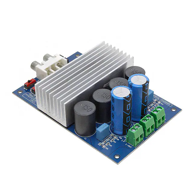
-
STEVAL-CCA044V1
STMicroelectronics
-
93105
MISCO
-
93103
MISCO
-
1752
Adafruit Industries LLC
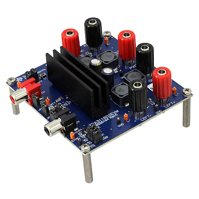
-
TPA3116D2EVM
Texas Instruments
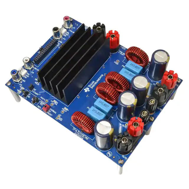
-
TPA3255EVM
Texas Instruments
Tech Hub

A practical engineering and sourcing framework covering lifecycle verification, lifetime-buy calculations, replacement qualification, supplier checks and counterfeit-risk controls.

TTL and CMOS logic families differ in thresholds, loading, output drive, power and timing. This engineering guide compares 74HC and 74HCT, calculates noise margins and checks 3.3 V/5 V compatibility.

A practical engineering guide to 3.3V and 5V logic compatibility, input thresholds, resistor dividers, translator ICs, MOSFET level shifting, I2C pull-ups, timing limits and power-sequencing risks.

The 74HC595 uses push-pull logic outputs, while the TPIC6B595 uses 50 V open-drain DMOS sinks for higher-power loads. This guide compares timing, current limits, 3.3 V interfacing, load wiring, thermal…

The 74HC595 converts serial data into eight stable parallel outputs. This guide covers pin functions, shift and storage timing, OE and MR behavior, drive-current limits, cascading, voltage compatibilit…

A technical comparison of level-sensitive latches and edge-triggered flip-flops, covering timing windows, setup and hold limits, master–slave operation, time borrowing, race-through, HDL inference and…

A D latch stores one bit while Enable controls when data can pass. This reference covers gate-level operation, truth tables, transparency, setup and hold timing, LE versus OE, common ICs and practical …

An SR latch stores one bit through cross-coupled feedback. This engineering reference covers NOR and NAND implementations, truth tables, forbidden-state recovery, gated operation, switch debouncing, fa…

Latch circuits retain one bit through feedback. This technical reference covers SR and D latches, truth tables, transparency, timing limits, latch-versus-flip-flop behavior, applications and common log…

An engineering guide to LED driver operation, constant-current and constant-voltage outputs, linear and switching topologies, dimming, IC selection, calculations, replacement compatibility, and fault c…


