
 My Inquiry
 My Account


Renesas DF3067RX20V
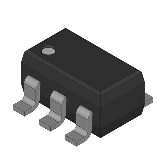
- Part No.:
- DF3067RX20V
- Manufacturer:
- Renesas
- Category:
- Microcontrollers
- Package:
- -
- Datasheet:
-
 DF3067RX20V.pdf
- Description:
- IC MCU 16BIT 128KB FLASH
- Quantity:
- Payment:

- Shipping:

Inventory:104
Please send an inquiry. Send us your inquiry, and we will respond immediately.
Product details
Overview
DF3067RX20V from Maxim Integrated is a factory-trimmed 3-pin silicon oscillator delivering a precise 12MHz rail-to-rail square-wave clock output with ±2% initial accuracy, 5µs startup time, and ±100ppm/°C temperature drift-designed as a robust, vibration- and EMI-resistant replacement for ceramic resonators and crystal oscillators in microcontroller and UART clocking applications operating from 2.7V to 5.5V.
For engineers reviewing the DF3067RX20V datasheet, DF3067RX20V pinout, DF3067RX20V application, or DF3067RX20V equivalent, this device offers plug-in compatibility with standard SC70-3 footprints, no external load capacitors, fast startup under wide temperature (-40°C to +125°C), and low jitter (180psP-P at 16MHz) - critical for timing-sensitive embedded control and automotive systems.
Technical Context
The DF3067RX20V implements a fully integrated, PLL-free oscillator core using BiCMOS process technology, generating stable frequency directly without feedback loops or external tuning components. Its push-pull CMOS output drives 1kΩ to GND or 500Ω to V+ while maintaining 40–60% duty cycle across supply (2.7V–5.5V) and temperature (-40°C to +125°C).
It eliminates high-impedance nodes and crystal-mounting sensitivity, making it inherently resistant to mechanical shock, board-level EMI, and humidity-induced frequency shift. Startup occurs within 5µs after V+ exceeds 1.65V, and output rise/fall times are tightly controlled at 5ns (CL = 10pF).
Key Specifications
| Parameter | Value and Actual Design Meaning |
|---|---|
| Output Frequency | 12MHz nominal - factory-trimmed, no calibration required; matches standard µC/UART clock requirements. |
| Initial Accuracy | ±2% at +25°C - enables reliable boot timing without post-manufacture trimming. |
| Temp Drift | ±100ppm/°C - ensures <±0.12% frequency deviation over full -40°C to +125°C range. |
| Startup Time | 5µs - allows immediate system clock availability after power ramp, reducing reset delay. |
| Supply Range | 2.7V to 5.5V - supports direct interface with 3.3V and 5V logic domains without level shifting. |
| Output Drive | ±10mA - drives heavy capacitive loads (up to 100pF) without buffer, simplifying layout. |
| Jitter (16MHz) | 180psP-P - meets timing margin requirements for high-speed serial interfaces (e.g., UART at 3Mbps). |
Pinout & Package
DF3067RX20V is housed in a space-saving 3-pin SC70-3 package (2.0mm × 2.1mm × 0.9mm), optimized for high-density PCB layouts and reflow-compatible assembly.
| Pin/Terminal | Circuit Role | Design Meaning |
|---|---|---|
| V+ | Positive supply input | Accepts 2.7V–5.5V; requires local 0.1µF ceramic bypass to GND for noise immunity. |
| CLOCK | CMOS push-pull clock output | Directly drives µC/UART clock input; no series resistor or termination needed. |
| GND | Ground reference | Must be connected to system ground plane; forms return path for output current. |
Key Features
| Feature | Design Value |
|---|---|
| No external components | Eliminates load capacitors, bias resistors, and feedback networks - reduces BOM count and layout area. |
| Vibration/EMI immunity | Robust operation in harsh environments (e.g., engine control units) due to solid-state design and absence of piezoelectric elements. |
| Rail-to-rail 50% duty cycle | Ensures balanced high/low time for synchronous logic, minimizing setup/hold violations in µC peripherals. |
| Fast 5µs startup | Enables immediate clock availability after power-on, supporting deterministic boot sequences in safety-critical systems. |
| -40°C to +125°C operation | Guaranteed performance across automotive and industrial temperature ranges without derating. |
Applications
| Automotive Body Control Module | Industrial PLC Timing Reference |
|---|---|
Use Scenario: Clock source for 8-bit/32-bit MCUs managing door locks, lighting, and sensor polling in vehicle body electronics. IC Role / Device Role / Timing Role: Primary system clock generator replacing quartz crystals vulnerable to road vibration and thermal cycling. Use Value: Eliminates crystal microfracture risk and frequency drift under 5g shock, improving long-term timing reliability. |
Use Scenario: Synchronizing I/O scan cycles and communication stacks (e.g., Modbus RTU) in DIN-rail mounted programmable logic controllers. IC Role / Device Role / Timing Role: Stable, low-jitter timing reference ensuring deterministic execution timing across temperature swings. Use Value: Maintains ±100ppm/°C stability over -40°C to +85°C ambient, preventing scan-time jitter that could trigger watchdog timeouts. |
| White Goods Mainboard MCU | Handheld Medical Device Clock |
Use Scenario: Providing clock signal to ARM Cortex-M0+ MCU controlling washing machine motor sequencing, water heating, and display UI. IC Role / Device Role / Timing Role: System clock generator tolerant to humid, condensing environments inside appliance enclosures. Use Value: No high-impedance nodes prevents moisture-induced leakage paths - avoids clock stoppage during steam exposure. |
Use Scenario: Timing source for low-power BLE-enabled glucose meter MCU performing ADC sampling and wireless transmission. IC Role / Device Role / Timing Role: Low-jitter, fast-start oscillator enabling rapid wake-from-sleep clock recovery for battery-efficient operation. Use Value: 5µs startup and 180psP-P jitter support sub-millisecond measurement windows with <1 LSB timing error in 12-bit ADC sampling. |
Equivalent & Alternatives
The following parts are listed as comparable options for similar silicon oscillator applications.
| Alternative Part | Technical Difference | Application Difference | Selection Advice |
|---|---|---|---|
| SiT1533AI-H4-33E-12.000000 | MEMS-based; ±10ppm initial accuracy; 1.62–3.63V supply; 1.2µA standby current | Better accuracy and lower power, but higher cost and longer lead time; requires different footprint (2.0mm × 1.2mm DFN) | Select when ultra-low power or tight frequency tolerance is prioritized over cost and drop-in replacement. |
| ABM3B-12.000MHZ-D2Y-T | Quartz crystal + internal oscillator IC; ±10ppm accuracy; 1.8–3.3V only; 3.5mA typical supply current | Higher EMI susceptibility and mechanical fragility; limited to low-voltage systems; needs external load caps | Choose only if legacy design mandates quartz-based timing or existing layout accommodates 4-pin SMD crystal footprint. |
Compared with DF3067RX20V, SiT1533AI-H4-33E-12.000000 offers superior accuracy and power efficiency but lacks pin compatibility and adds MEMS-specific qualification overhead; ABM3B-12.000MHZ-D2Y-T provides quartz-grade stability but introduces vibration sensitivity and voltage-range limitations - DF3067RX20V balances ruggedness, simplicity, and broad supply compatibility.
Availability
DF3067RX20V is available at Aetrix Electronics and suitable for automotive body control modules, industrial PLC timing references, and white goods mainboard MCU applications requiring stable component supply, extended temperature operation, and vibration-immune clock generation.
Supply support for DF3067RX20V includes scheduled delivery planning, volume procurement assistance, BOM continuity management, traceable sourcing, and lifecycle availability coordination for OEM customers, industrial embedded developers, connected-device designers, and electronics production programs.
Manufacturer
Maxim Integrated (now part of Analog Devices) designs precision analog, mixed-signal, and timing solutions for demanding industrial, automotive, and computing applications - emphasizing reliability, integration, and environmental robustness.
DF3067RX20V belongs to Maxim's silicon oscillator product line, engineered to replace fragile quartz and ceramic timing elements with monolithic, EMI-hardened alternatives for mission-critical embedded clocking.
FAQ
What is the exact output frequency and tolerance of DF3067RX20V?
The DF3067RX20V is factory-trimmed to deliver a nominal 12MHz output frequency with ±2% initial accuracy at +25°C. Over the full -40°C to +125°C operating range, frequency variation remains within ±0.12% due to its specified ±100ppm/°C temperature coefficient. This makes DF3067RX20V suitable for applications where crystal-level stability is unnecessary but robustness is essential.
Does DF3067RX20V require external load capacitors or biasing components?
No - DF3067RX20V is a fully integrated oscillator requiring zero external components. Unlike quartz crystals or ceramic resonators, it does not need load capacitors, feedback resistors, or gain-setting networks. The only recommended external component is a 0.1µF ceramic bypass capacitor between V+ and GND, placed adjacent to the device to ensure power-supply noise rejection.
Can DF3067RX20V directly drive a microcontroller clock input?
Yes - DF3067RX20V features a rail-to-rail CMOS push-pull output capable of directly driving standard µC clock inputs (e.g., STM32, PIC, or NXP Kinetis families) without level-shifting or series termination. Its ±10mA drive strength supports capacitive loads up to 100pF, and its 40–60% duty cycle meets typical MCU clock input requirements for balanced timing margins.
How does DF3067RX20V perform under mechanical vibration or EMI exposure?
DF3067RX20V exhibits exceptional immunity to vibration and EMI because it contains no piezoelectric elements or high-impedance nodes. Its solid-state BiCMOS oscillator core eliminates microfracture risks associated with quartz crystals and avoids frequency pulling caused by nearby RF fields - validated in automotive-grade testing per AEC-Q200 guidelines for harsh environment operation.
What is the startup behavior of DF3067RX20V after power application?
DF3067RX20V achieves stable clock output within 5µs after V+ rises above 1.65V (at +25°C). For reliable system initialization, it is recommended to assert MCU reset until at least 20µs after V+ exceeds 2.7V. This behavior is consistent across the full supply range (2.7V–5.5V) and temperature range (-40°C to +125°C), making DF3067RX20V ideal for fast-boot embedded systems.
DF3067RX20V Specifications
- Product attributes
- Attribute value
- Manufacturer:
- Renesas
- Package/Case:
- -
- Series:
- H8® H8/300H
- Packaging:
- Bulk
- Product Status:
- Active
- Programmable:
- Not Verified
- Core Processor:
- H8/300H
- Core Size:
- 16-Bit
- Speed:
- 20MHz
- Connectivity:
- -
- Peripherals:
- DMA, PWM, WDT
- Number of I/O:
- 70
- Program Memory Size:
- 128KB (128K x 8)
- Program Memory Type:
- FLASH
- EEPROM Size:
- -
- RAM Size:
- 4K x 8
- Voltage - Supply (Vcc/Vdd):
- 4.5V ~ 5.5V
- Data Converters:
- A/D 8x10b; D/A 2x8b
- Oscillator Type:
- Internal
- Operating Temperature:
- -20°C ~ 75°C (TA)
- Grade:
- -
- Qualification:
- -
- Mounting Type:
- -
- Supplier Device Package:
DF3067RX20V FAQ
1.How can I place an order for DF3067RX20V through Aetrix?
Please submit a Request for Quotation (RFQ) for DF3067RX20V on Aetrix. Our sales agent will provide a competitive quotation and guide you through the order confirmation once you accept the terms.
2.Are the price and stock information for DF3067RX20V reliable?
The price and inventory of DF3067RX20V are updated periodically and may fluctuate due to market conditions. Stock and pricing data are typically refreshed every 24 hours. Quotation validity for DF3067RX20V is usually 5 days.
3.What payment methods are accepted for DF3067RX20V?
We accept Wire Transfer, PayPal, Credit Card, Western Union, MoneyGram, and Escrow for DF3067RX20V transactions.
Note: Certain payment methods may incur a processing fee.
4.How is shipping managed for DF3067RX20V?
DF3067RX20V orders can be shipped via leading logistics carriers, including DHL, UPS, FedEx, TNT, or Registered Mail.
Once your DF3067RX20V order is processed, you will receive an email with the shipment details and tracking number.
Note: Tracking information may take up to 24 hours to appear. Express delivery typically takes 3–5 business days.
5.How can I obtain technical support or documentation for DF3067RX20V?
For technical support, including DF3067RX20V datasheets, pinout diagrams, or application guidance, please contact our engineering support team. They can provide detailed documentation and assistance for your DF3067RX20V requirements.
6.How does Aetrix verify that DF3067RX20V is sourced from the original manufacturer or authorized distributors?
All DF3067RX20V products on Aetrix are procured from qualified distributors and authorized channels. Our dedicated quality assurance team conducts strict verification, including traceability checks and, if necessary, third-party testing. This ensures that DF3067RX20V meets industry standards.
7.What is the process for return or replacement of DF3067RX20V?
All DF3067RX20V units undergo pre-shipment inspection (PSI). If there is an issue with DF3067RX20V, returns or replacements are accepted under the following conditions:
1.Quantity discrepancies, incorrect items, or visible external defects (such as breakage or corrosion), acknowledged by Aetrix.
2.The issue is reported within 90 days of delivery.
3.The DF3067RX20V part is unused and in its original packaging.
Return procedure for DF3067RX20V:
1.Submit a request within 90 days.
2.Obtain a Return Material Authorization (RMA) from Aetrix.
DF3067RX20V Tags

-
ATTINY4-TSHR
Microchip Technology
-
ATTINY10-TSHR
Microchip Technology
-
ATTINY10-TS8R
Microchip Technology

-
ATTINY202-SSNR
Microchip Technology
-
ATTINY202-SSFR
Microchip Technology
-
ATTINY402-SSNR
Microchip Technology

-
PIC16F15213T-I/MF
Microchip Technology
-
PIC16F15213-E/MF
Microchip Technology

-
PIC10F200T-I/OT
Microchip Technology
-
ATTINY412-SSNR
Microchip Technology
-
PIC10F202T-I/OT
Microchip Technology

-
ATTINY404-SSNR
Microchip Technology
Tech Hub

TTL and CMOS logic families differ in thresholds, loading, output drive, power and timing. This engineering guide compares 74HC and 74HCT, calculates noise margins and checks 3.3 V/5 V compatibility.

A practical engineering guide to 3.3V and 5V logic compatibility, input thresholds, resistor dividers, translator ICs, MOSFET level shifting, I2C pull-ups, timing limits and power-sequencing risks.

The 74HC595 uses push-pull logic outputs, while the TPIC6B595 uses 50 V open-drain DMOS sinks for higher-power loads. This guide compares timing, current limits, 3.3 V interfacing, load wiring, thermal…

The 74HC595 converts serial data into eight stable parallel outputs. This guide covers pin functions, shift and storage timing, OE and MR behavior, drive-current limits, cascading, voltage compatibilit…

A technical comparison of level-sensitive latches and edge-triggered flip-flops, covering timing windows, setup and hold limits, master–slave operation, time borrowing, race-through, HDL inference and…

A D latch stores one bit while Enable controls when data can pass. This reference covers gate-level operation, truth tables, transparency, setup and hold timing, LE versus OE, common ICs and practical …

An SR latch stores one bit through cross-coupled feedback. This engineering reference covers NOR and NAND implementations, truth tables, forbidden-state recovery, gated operation, switch debouncing, fa…

Latch circuits retain one bit through feedback. This technical reference covers SR and D latches, truth tables, transparency, timing limits, latch-versus-flip-flop behavior, applications and common log…

An engineering guide to LED driver operation, constant-current and constant-voltage outputs, linear and switching topologies, dimming, IC selection, calculations, replacement compatibility, and fault c…

Operational amplifier guide covering op amp basics, feedback, ideal vs real op amps, common configurations, buffer circuits, offset, bias current, gain-bandwidth, slew rate, rail-to-rail limits and sel…


