Send an Inquiry

To receive a quote for your project, please fill in the following information, and we’ll get back to you promptly.

Name*
Company*
Email Address*
Phone/WhatsApp
Part Number*
Quantity*
Message
Submit Inventory List

Please fill in the following information, and we’ll get back to you promptly.

Name*
Company*
Email Address*
Phone/WhatsApp
Upload My List
Message

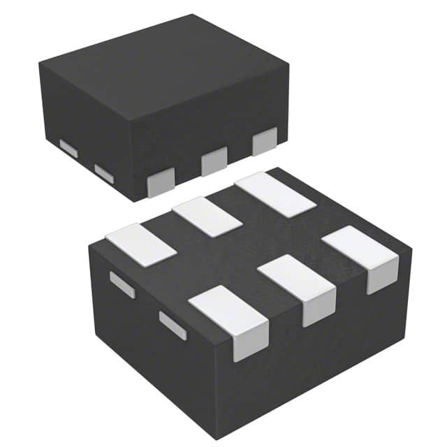
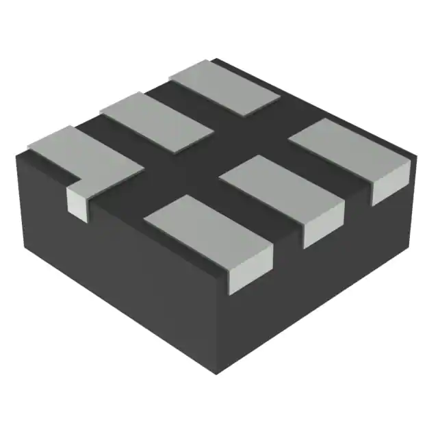
Vishay Siliconix DG2512DN-T1-E4

Part No.:
DG2512DN-T1-E4
Manufacturer:
Vishay Siliconix
Category:
Analog Switches, Multiplexers, Demultiplexers
Package:
6-UFDFN
Datasheet:
AetrixDG2512DN-T1-E4.pdf
Description:
IC SW SPST-NCX1 1.3OHM 6MINIQFN
Quantity:
Payment:
Payment
Shipping:
Shipping

Inventory:1,992

Please send an inquiry. Send us your inquiry, and we will respond immediately.

Part Number
Quantity*
Price
Name*
Company
Email*
Comments

Product details

Overview

DG2512DN-T1-E4 from Vishay Siliconix is a low-voltage, single-pole/single-throw (SPST) monolithic CMOS analog switch in miniQFN-6 package, featuring 1.3 Ω on-resistance at 2.7 V, 1.8 V to 5.5 V supply range, and guaranteed break-before-make timing. It serves as a bidirectional signal path selector in portable battery-powered systems requiring minimal board space and low power consumption.

For engineers reviewing the DG2512DN-T1-E4 datasheet, DG2512DN-T1-E4 pinout, DG2512DN-T1-E4 application, or DG2512DN-T1-E4 equivalent, key selection criteria include on-resistance flatness (≤0.4 Ω), charge injection (3 pC typ. at 2.7 V), off-isolation (–58 dB), and compatibility with 1.8 V logic control in space-constrained analog signal routing.

Technical Context

The DG2512DN-T1-E4 implements a single SPST switch with true bidirectional conduction and rail-to-rail analog signal handling (0 V to V+). Its JI5L low-voltage CMOS process ensures latch-up immunity (>300 mA per JESD78A) and supports operation down to 1.8 V while maintaining sub-2 Ω RON across –40 °C to +85 °C.

Break-before-make timing is guaranteed (1–12 ns), preventing momentary shorting during state transitions. The device uses internal clamping diodes to protect NC/NO/COM pins against overvoltage up to V+ + 0.3 V, with leakage currents limited to ±20 nA across temperature and supply conditions.

Key Specifications

Parameter Value and Actual Design Meaning
Supply Voltage Range 1.8 V to 5.5 V - enables direct interface with 1.8 V, 2.5 V, 3.3 V, and 5 V logic and analog rails without level shifting.
On-Resistance (RON) 1.3 Ω typ. at 2.7 V - minimizes signal attenuation and voltage drop in precision analog paths (e.g., sensor front-ends).
RON Flatness ≤0.4 Ω - ensures consistent gain and linearity across full analog input range (0 V to V+), critical for ADC/DAC multiplexing.
Charge Injection 3 pC typ. at 2.7 V - reduces sampling error and settling time in sample-and-hold and data acquisition circuits.
Off-Isolation (OIRR) –58 dB at 1 MHz - suppresses crosstalk between adjacent channels in multi-signal routing applications.
Turn-On/Off Time 18 ns / 7 ns typ. at 2.7 V - supports high-speed switching in portable comms and test equipment signal paths.
Input Logic Thresholds VINH = 1.6 V min., VINL = 0.4 V max. at 3 V - ensures reliable TTL/CMOS-compatible control with margin at low supply.

Pinout & Package

Package: miniQFN-6 (1.2 mm × 1.0 mm, 0.4 mm pitch, 0.55 mm height), Pb-free with NiPdAu terminations (–E4 suffix), thermally enhanced exposed pad (pin 6 = GND).

Pin/Terminal Circuit Role Design Meaning
1 (IN) Digital control input Active-high logic input; drives internal CMOS gate; compatible with 1.8 V logic thresholds.
2 (GND) Ground reference Analog and digital ground return; must be connected to system ground plane for noise immunity.
3 (COM) Common analog terminal Bidirectional signal path; connects to source or load depending on switch state; handles full rail-to-rail analog swing.
4 (NC) No-connect terminal Internally unconnected; must be left floating or tied to GND per layout best practice-no functional role.
5 (V+) Positive supply rail Provides power for analog switch core and level-shifting circuitry; decoupling capacitor required near pin.
6 (Exposed Pad) Thermal & electrical GND Integral thermal path to PCB; must be soldered to solid GND copper area for thermal dissipation and EMI reduction.

Key Features

Feature Design Value
Low on-resistance flatness 0.4 Ω max. variation across analog voltage range - preserves signal integrity in precision instrumentation and audio routing.
Guaranteed break-before-make 1–12 ns minimum interval - eliminates signal shorting during channel switching in multiplexer-based data acquisition.
Latch-up immunity >300 mA per JESD78A - ensures robust operation under transient overcurrent events in portable electronics.
Ultra-low charge injection 3 pC typical - enables accurate sampling in high-resolution SAR ADC interfaces without added correction circuitry.
Miniature footprint 1.2 mm × 1.0 mm - saves >60% board area vs. comparable SC-70 or SOT-363 switches, critical for ultra-thin mobile designs.

Applications

Portable Test Equipment Cellular Phone Front-End

Use Scenario: Signal routing between multiple sensor inputs and a shared ADC in handheld multimeters or calibrators.

IC Role / Device Role / Timing Role: SPST analog switch enabling sequential sampling of thermocouples, RTDs, and voltage sources with minimal crosstalk.

Use Value: 1.3 Ω RON and –58 dB off-isolation maintain measurement accuracy across 16-bit dynamic range without calibration drift.

Use Scenario: Antenna switching and RF front-end signal path selection in LTE/Wi-Fi combo modules.

IC Role / Device Role / Timing Role: Low-capacitance (21 pF off-state), fast-switching (18 ns tON) SPST switch isolating PA output from antenna diversity paths.

Use Value: 3 pC charge injection prevents DC offset in sensitive LNA bias networks; 1.8 V operation aligns with baseband processor I/O voltage.

Low-Voltage Data Acquisition ADC/DAC Multiplexing

Use Scenario: Battery-powered environmental monitoring node aggregating temperature, humidity, and gas sensor outputs.

IC Role / Device Role / Timing Role: Rail-to-rail analog switch supporting 0–3.3 V sensor signals while operating from same 3.3 V supply as microcontroller.

Use Value: 1.8 V minimum supply allows extended runtime in deep-discharge states; <20 nA leakage preserves sensor bias stability.

Use Scenario: Channel selection in 12-bit SAR ADC subsystems with multiple analog inputs (e.g., industrial PLC analog I/O).

IC Role / Device Role / Timing Role: Precision SPST switch providing matched RON and low flatness to minimize gain error across all channels.

Use Value: ≤0.4 Ω RON flatness ensures <0.02% gain nonlinearity; 61 pF on-capacitance avoids bandwidth degradation at 1 MSPS sampling rates.

Equivalent & Alternatives

The following parts are listed as comparable options for similar SPST analog switch applications.

Alternative Part Technical Difference Application Difference Selection Advice
Texas Instruments TS5A23157DBVR RON = 0.9 Ω typ. at 3 V; 1.65–5.5 V supply; no guaranteed break-before-make; 6-pin SOT-23 package (2.9 mm × 1.6 mm). Larger footprint; higher RON flatness (0.7 Ω); lacks BBM guarantee - less suitable for precision multiplexing where channel shorting must be avoided. Prefer DG2512DN-T1-E4 when board space is constrained or BBM timing is mandatory; choose TS5A23157DBVR only if lower RON outweighs size and timing risk.
Analog Devices ADG801BRMZ-REEL7 RON = 0.3 Ω typ. at 3 V; 1.8–5.5 V supply; 6-pin MSOP package (3.0 mm × 3.0 mm); 15 pC charge injection. 3× larger footprint; 5× higher charge injection; higher cost; better RON but worse signal integrity in sampling applications. Select DG2512DN-T1-E4 for portable, low-power, space-sensitive designs needing low QINJ and minimal board area; ADG801BRMZ-REEL7 fits only where ultra-low RON justifies size and cost penalties.

Compared with TS5A23157DBVR and ADG801BRMZ-REEL7, the DG2512DN-T1-E4 delivers optimal balance of miniature size (1.2 × 1.0 mm), guaranteed break-before-make, and ultra-low charge injection (3 pC) - making it uniquely suited for battery-powered precision signal routing where layout area and sampling fidelity are co-constrained.

Availability

DG2512DN-T1-E4 is available at Aetrix Electronics and suitable for portable test equipment, cellular phone front-end modules, and low-voltage data acquisition systems requiring stable component supply, long-term lifecycle support, and RoHS-compliant manufacturing.

Supply support for DG2512DN-T1-E4 includes scheduled delivery planning, volume procurement assistance, BOM continuity management, traceable sourcing, and lifecycle availability coordination for OEM customers, industrial embedded developers, connected-device designers, and electronics production programs.

Manufacturer

Vishay Siliconix is a global leader in discrete semiconductors and passive components, specializing in high-reliability, high-performance analog solutions for industrial, automotive, and consumer markets.

The DG2512DN-T1-E4 belongs to Vishay's low-voltage analog switch family built on the JI5L process, designed specifically for space- and power-constrained portable electronics requiring rail-to-rail signal handling and robust latch-up immunity.

FAQ

What is the maximum analog signal voltage range supported by the DG2512DN-T1-E4?

The DG2512DN-T1-E4 supports analog signals from 0 V to V+, where V+ ranges from 1.8 V to 5.5 V. For example, with V+ = 3.3 V, the COM, NC, and NO pins handle signals from 0 V to 3.3 V continuously. Signals exceeding V+ + 0.3 V are clamped by internal diodes, so external protection is recommended beyond that limit. This rail-to-rail capability makes the DG2512DN-T1-E4 ideal for interfacing with modern low-voltage sensors and ADCs without level-shifting circuitry.

Does the DG2512DN-T1-E4 require external pull-up or pull-down resistors on the IN pin?

No, the DG2512DN-T1-E4 does not require external pull-up or pull-down resistors on the IN pin. Its input structure accepts 1.8 V logic levels directly: VINH is guaranteed ≥1.6 V and VINL ≤0.4 V at 3 V supply, providing sufficient noise margin for clean switching. Input current remains below 1 µA across temperature, eliminating static loading concerns. However, in noisy environments or floating-control scenarios, a 100 kΩ pull-down is recommended to ensure defined state during power-up or MCU reset - but this is a system-level design choice, not a requirement of the DG2512DN-T1-E4 itself.

How is thermal performance managed in the miniQFN-6 package of the DG2512DN-T1-E4?

The DG2512DN-T1-E4's miniQFN-6 package features an exposed thermal pad (pin 6) that must be soldered to a dedicated GND copper pour on the PCB to achieve rated thermal performance. With proper layout - including ≥4 thermal vias under the pad connected to inner-layer GND planes - the device maintains junction temperatures within specification even at 150 mA continuous current. Derating begins above 70 °C (2 mW/°C), and maximum power dissipation is 160 mW. This thermal design enables reliable operation in sealed portable enclosures without forced airflow.

Can the DG2512DN-T1-E4 be used in bidirectional signal paths such as I²C or UART lines?

The DG2512DN-T1-E4 supports true bidirectional analog conduction when ON, but it is not recommended for digital bus isolation like I²C or UART. Its 61 pF on-capacitance and lack of bus-specific features (e.g., slew rate control, fail-safe biasing, or ESD rating beyond standard HBM) limit speed and noise immunity in open-drain or push-pull digital protocols. It is optimized for analog signal routing - e.g., sensor multiplexing or audio path selection - where signal integrity, low RON, and low charge injection matter more than digital timing margins. For digital buses, purpose-built bus switches (e.g., TS3A226AE) are preferred.

What is the significance of the "-E4" suffix in DG2512DN-T1-E4?

The "-E4" suffix in DG2512DN-T1-E4 indicates Vishay's lead (Pb)-free construction with NiPdAu (nickel-palladium-gold) device terminations, compliant with RoHS Directive 2011/65/EU. This suffix replaces older Pb-containing variants and ensures compatibility with modern reflow profiles and environmental requirements. The "DN" denotes miniQFN-6 packaging, "T1" specifies tape-and-reel delivery (3,000 units per reel), and the full part number DG2512DN-T1-E4 is orderable and traceable through Vishay's authorized distribution network. No functional or electrical differences exist between -E4 and legacy versions beyond termination material.

DG2512DN-T1-E4 Specifications

Product attributes
Attribute value
Manufacturer:
Vishay Siliconix
Series:
-
Packaging:
Tape & Reel (TR)
Product Status:
Obsolete
Switch Circuit:
SPST - NC
Multiplexer/Demultiplexer Circuit:
1:1
Number of Circuits:
1
On-State Resistance (Max):
1.3Ohm
Channel-to-Channel Matching (ΔRon):
150mOhm (Max)
Voltage - Supply, Single (V+):
1.8V ~ 5.5V
Voltage - Supply, Dual (V±):
-
Switch Time (Ton, Toff) (Max):
35ns, 31ns
-3db Bandwidth:
-
Charge Injection:
14pC
Channel Capacitance (CS(off), CD(off)):
19pF
Current - Leakage (IS(off)) (Max):
2nA
Crosstalk:
-64dB @ 1MHz
Operating Temperature:
-40°C ~ 85°C (TA)
Grade:
-
Qualification:
-
Mounting Type:
Surface Mount
Supplier Device Package:
6-miniQFN (1x1.2)

DG2512DN-T1-E4 FAQ

1.How can I place an order for DG2512DN-T1-E4 through Aetrix?

Please submit a Request for Quotation (RFQ) for DG2512DN-T1-E4 on Aetrix. Our sales agent will provide a competitive quotation and guide you through the order confirmation once you accept the terms.

2.Are the price and stock information for DG2512DN-T1-E4 reliable?

The price and inventory of DG2512DN-T1-E4 are updated periodically and may fluctuate due to market conditions. Stock and pricing data are typically refreshed every 24 hours. Quotation validity for DG2512DN-T1-E4 is usually 5 days.

3.What payment methods are accepted for DG2512DN-T1-E4?

We accept Wire Transfer, PayPal, Credit Card, Western Union, MoneyGram, and Escrow for DG2512DN-T1-E4 transactions.

Note: Certain payment methods may incur a processing fee.

4.How is shipping managed for DG2512DN-T1-E4?

DG2512DN-T1-E4 orders can be shipped via leading logistics carriers, including DHL, UPS, FedEx, TNT, or Registered Mail.

Once your DG2512DN-T1-E4 order is processed, you will receive an email with the shipment details and tracking number.

Note: Tracking information may take up to 24 hours to appear. Express delivery typically takes 3–5 business days.

5.How can I obtain technical support or documentation for DG2512DN-T1-E4?

For technical support, including DG2512DN-T1-E4 datasheets, pinout diagrams, or application guidance, please contact our engineering support team. They can provide detailed documentation and assistance for your DG2512DN-T1-E4 requirements.

6.How does Aetrix verify that DG2512DN-T1-E4 is sourced from the original manufacturer or authorized distributors?

All DG2512DN-T1-E4 products on Aetrix are procured from qualified distributors and authorized channels. Our dedicated quality assurance team conducts strict verification, including traceability checks and, if necessary, third-party testing. This ensures that DG2512DN-T1-E4 meets industry standards.

7.What is the process for return or replacement of DG2512DN-T1-E4?

All DG2512DN-T1-E4 units undergo pre-shipment inspection (PSI). If there is an issue with DG2512DN-T1-E4, returns or replacements are accepted under the following conditions:

1.Quantity discrepancies, incorrect items, or visible external defects (such as breakage or corrosion), acknowledged by Aetrix.

2.The issue is reported within 90 days of delivery.

3.The DG2512DN-T1-E4 part is unused and in its original packaging.

Return procedure for DG2512DN-T1-E4:

1.Submit a request within 90 days.

2.Obtain a Return Material Authorization (RMA) from Aetrix.

DG2512DN-T1-E4 Tags

  • DG2512DN-T1-E4
  • DG2512DN-T1-E4 PDF
  • DG2512DN-T1-E4 Datasheet
  • DG2512DN-T1-E4 Specifications
  • DG2512DN-T1-E4 Images
  • Vishay Siliconix
  • Vishay Siliconix DG2512DN-T1-E4
  • Buy DG2512DN-T1-E4
  • DG2512DN-T1-E4 Price
  • DG2512DN-T1-E4 Distributor
  • DG2512DN-T1-E4 Supplier
  • DG2512DN-T1-E4 Wholesale
Related Products
SN74LVC1G3157DBVR
SN74LVC1G3157DBVR

Texas Instruments

SN74LVC1G66DBVR
SN74LVC1G66DBVR

Texas Instruments

SN74LVC1G66DCKR
SN74LVC1G66DCKR

Texas Instruments

SN74LVC1G3157DSFR
SN74LVC1G3157DSFR

Texas Instruments

1P1G3157QDCKRQ1
1P1G3157QDCKRQ1

Texas Instruments

SN74LVC2G66DCUR
SN74LVC2G66DCUR

Texas Instruments

SN74LV4052APWR
SN74LV4052APWR

Texas Instruments

74HC4051D,653
74HC4051D,653

Nexperia USA Inc.

SN74LV4051APWR
SN74LV4051APWR

Texas Instruments

CD74HC4052PWR
CD74HC4052PWR

Texas Instruments

CD74HC4051PWR
CD74HC4051PWR

Texas Instruments

TS5A3166DBVR
TS5A3166DBVR

Texas Instruments

Tech Hub

Search

Search

PRODUCT

PRODUCT

PHONE

PHONE

USER

USER