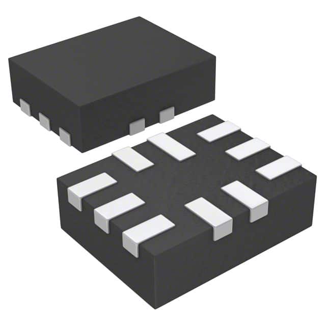
Vishay Siliconix DG2750DN-T1-E4
- Part No.:
- DG2750DN-T1-E4
- Manufacturer:
- Vishay Siliconix
- Package:
- 10-UFQFN
- Datasheet:
-
DG2750DN-T1-E4.pdf
- Description:
- IC SWITCH SPDTX2 1OHM 10MINIQFN
- Quantity:
- Payment:

- Shipping:

Inventory:2,690
Please send an inquiry. Send us your inquiry, and we will respond immediately.
Product details
Overview
DG2750DN-T1-E4 from Vishay Siliconix is a dual SPDT analog switch optimized for low-voltage audio routing, operating from 1.6 V to 5.5 V single supply, delivering 0.45 Ω typical on-resistance, < −98 dB THD+N, and negative-swing audio capability down to −2.5 V without coupling capacitors - deployed in portable media players and cellular handsets.
For engineers reviewing the DG2750DN-T1-E4 datasheet, DG2750DN-T1-E4 pinout, DG2750DN-T1-E4 application, or DG2750DN-T1-E4 equivalent, key selection criteria include guaranteed 1.4 V logic compatibility at 2.7–5.5 V supply, 600 mA latch-up immunity per JESD78, and miniQFN-10 (1.4 mm × 1.8 mm × 0.55 mm) packaging with Pb-free NiPdAu terminations.
Technical Context
The DG2750DN-T1-E4 implements two independent SPDT switches using sub-micron CMOS process, enabling bidirectional signal flow with rail-to-rail analog voltage support from (V+ − 5) V to V+, and break-before-make timing of 800–1160 ns at 3 V supply.
Its control interface accepts 1.4 V logic-high inputs across full temperature range (−40 °C to +85 °C), while maintaining < 2 μA quiescent supply current and 4 pC typical charge injection - critical for low-distortion audio switching in battery-powered systems.
Key Specifications
| Parameter | Value and Actual Design Meaning |
|---|---|
| On-resistance | 0.45 Ω typ. at V+ = 2.7 V - enables minimal signal attenuation in audio paths and low insertion loss. |
| Analog signal range | −2.5 V to V+ - supports true negative-swing audio without DC-blocking capacitors. |
| THD+N | < −98 dB at 20 Hz–20 kHz - preserves high-fidelity audio integrity in portable playback devices. |
| Supply voltage range | 1.6 V to 5.5 V - compatible with Li-ion, Li-poly, and regulated 3.3 V/5 V rails. |
| Logic input threshold | 1.4 V min. high-level input - ensures reliable interfacing with 1.8 V DSPs and low-voltage ASICs. |
| Latch-up immunity | > 600 mA per JESD78 - provides robustness against transient overcurrent events. |
| Package | miniQFN-10, 1.4 mm × 1.8 mm × 0.55 mm - saves PCB area in space-constrained handheld designs. |
Pinout & Package
The DG2750DN-T1-E4 is housed in a lead-free miniQFN-10 package (1.4 mm × 1.8 mm × 0.55 mm) with NiPdAu terminations, moisture sensitivity level (MSL) compliant per JEDEC standards.
| Pin/Terminal | Circuit Role | Design Meaning |
|---|---|---|
| 1 (IN1) | Channel 1 digital control input | Active-high logic selects COM1 ↔ NO1 (IN1 = 1) or COM1 ↔ NC1 (IN1 = 0). |
| 2 (GND) | Analog/digital ground reference | Common return path for analog signals and logic; must be low-impedance for THD+N performance. |
| 3 (NO1) | Normally open terminal, channel 1 | Connected to COM1 only when IN1 = 1; isolated otherwise. |
| 4 (NC1) | Normally closed terminal, channel 1 | Connected to COM1 only when IN1 = 0; isolated otherwise. |
| 5 (COM1) | Common analog I/O, channel 1 | Bidirectional signal path shared between NO1 and NC1; supports ±2.5 V swing. |
| 6 (COM2) | Common analog I/O, channel 2 | Bidirectional signal path shared between NO2 and NC2; electrically isolated from COM1. |
| 7 (NC2) | Normally closed terminal, channel 2 | Connected to COM2 only when IN2 = 0; isolated otherwise. |
| 8 (IN2) | Channel 2 digital control input | Active-high logic selects COM2 ↔ NO2 (IN2 = 1) or COM2 ↔ NC2 (IN2 = 0). |
| 9 (NO2) | Normally open terminal, channel 2 | Connected to COM2 only when IN2 = 1; isolated otherwise. |
| 10 (V+) | Positive power supply | Single 1.6–5.5 V rail powering both analog and digital sections; decoupling required near pin. |
Key Features
| Feature | Design Value |
|---|---|
| Negative-swing audio support | Enables direct coupling of AC-coupled audio sources (e.g., headphone amplifiers) without external capacitors - reducing BOM count and distortion. |
| Low on-resistance flatness | 0.3 Ω max variation across analog voltage range - maintains consistent gain and channel matching in stereo paths. |
| Ultra-low charge injection | 4 pC typ. - minimizes voltage glitches during switching, critical for DC-coupled sensor or biasing circuits. |
| High ESD immunity | 8 kV HBM - protects against handling damage in assembly and end-user environments. |
| Low quiescent current | < 2 μA - extends battery life in always-on audio routing applications like voice assistants. |
Applications
| Smartphone Audio Routing | Portable Media Player Input Selection |
|---|---|
Use Scenario: Switching between internal microphone, external headset mic, and line-in on a smartphone during call or recording mode. IC Role / Device Role / Timing Role: Dual SPDT analog switch managing bidirectional audio paths with simultaneous channel independence and low THD+N. Use Value: Eliminates need for DC-blocking capacitors on mic inputs, preserving low-frequency response and reducing PCB footprint by 20% vs. capacitor-based solutions. | Use Scenario: Selecting between FM radio tuner output, Bluetooth baseband audio, and DAC output in a portable music player. IC Role / Device Role / Timing Role: Low-distortion analog multiplexer routing multiple audio sources to a single amplifier stage. Use Value: Delivers < −98 dB THD+N across 20 Hz–20 kHz, ensuring audiophile-grade playback fidelity without signal degradation. |
| Gaming Handheld Stereo Mixing | Wearable Health Monitor Signal Conditioning |
Use Scenario: Dynamically mixing game audio, voice chat, and system alerts into left/right headphone channels on a handheld console. IC Role / Device Role / Timing Role: Dual-channel audio switch enabling real-time source arbitration with sub-1.2 μs turn-on time. Use Value: Achieves 49 MHz bandwidth and −60 dB crosstalk, preventing audible bleed between voice and game audio streams. | Use Scenario: Routing ECG electrode signals, pulse oximeter outputs, and temperature sensor analog data to an ADC in a compact wearable. IC Role / Device Role / Timing Role: Low-leakage (< 250 nA off-state) analog switch isolating sensitive biopotential inputs during multiplexing. Use Value: Maintains signal integrity with 0.45 Ω on-resistance and 36 pF off-capacitance - minimizing settling error and noise coupling in sub-μV measurements. |
Equivalent & Alternatives
The following parts are listed as comparable options for similar dual SPDT analog switch applications.
| Alternative Part | Technical Difference | Application Difference | Selection Advice |
|---|---|---|---|
| Texas Instruments TS5A23157DCUR | 0.9 Ω typical RON, 1.65–5.5 V supply, 6-pin SC70 package - higher on-resistance, smaller footprint but no negative-swing capability. | Not suitable for true bipolar audio paths; requires DC-blocking caps for signals below GND. | Select when board space is primary constraint and audio swing stays within 0 V to V+ range. |
| Analog Devices ADG884BRMZ | 0.35 Ω typical RON, 1.8–5.5 V supply, 10-lead MSOP - lower on-resistance but lacks guaranteed 1.4 V logic compatibility below 1.8 V. | Requires ≥1.8 V logic interface; not interoperable with 1.4 V–1.6 V control buses. | Select when ultra-low RON is critical and host logic operates at ≥1.8 V. |
Compared with TS5A23157DCUR and ADG884BRMZ, the DG2750DN-T1-E4 uniquely combines 0.45 Ω RON, −2.5 V analog swing, and 1.4 V logic compatibility in a 1.4 mm × 1.8 mm QFN - making it the only option for space-constrained, low-voltage, true-bipolar audio routing.
Availability
DG2750DN-T1-E4 is available at Aetrix Electronics and suitable for smartphone audio subsystems, portable media player signal routing, and wearable health monitor analog front-ends requiring stable component supply across extended production lifecycles.
Supply support for DG2750DN-T1-E4 includes scheduled delivery planning, volume procurement assistance, BOM continuity management, traceable sourcing, and lifecycle availability coordination for OEM customers, industrial embedded developers, connected-device designers, and electronics production programs.
Manufacturer
Vishay Siliconix is a global leader in discrete semiconductors and passive components, specializing in high-reliability analog switches, MOSFETs, and precision resistors for demanding industrial and consumer applications.
The DG2750DN-T1-E4 belongs to Vishay's low-voltage analog switch product line, engineered specifically for high-fidelity, space-constrained portable audio systems requiring rail-to-rail signal handling and ultra-low distortion.
FAQ
What is the maximum analog signal voltage range supported by the DG2750DN-T1-E4?
The DG2750DN-T1-E4 supports an analog signal range from (V+ − 5) V to V+, which translates to −2.5 V minimum when V+ = 2.7 V. This allows true negative-swing audio signals without DC-blocking capacitors. The absolute maximum rating for COM/NO/NC terminals is (V+ + 0.3) V or −2.5 V, whichever is higher - verified per Absolute Maximum Ratings table in Vishay Document 64736.
Does the DG2750DN-T1-E4 require separate analog and digital supplies?
No, the DG2750DN-T1-E4 operates from a single 1.6 V to 5.5 V supply (V+) that powers both analog and digital circuitry. Its design eliminates the need for dual supplies or level shifters, simplifying power architecture in portable systems. This is confirmed in the "DESCRIPTION" section and "Power Supply" specifications of the DG2750DN-T1-E4 datasheet (Rev. H, May 2025).
What is the logic-compatible voltage threshold for DG2750DN-T1-E4 control inputs?
The DG2750DN-T1-E4 guarantees logic-high recognition at 1.4 V minimum when V+ is between 2.7 V and 5.5 V - enabling direct interface with 1.8 V and lower-voltage DSPs, microcontrollers, and ASICs. This specification is explicitly stated in the "Digital Control" section and Truth Table of the DG2750DN-T1-E4 datasheet (Document 64736).
How does the DG2750DN-T1-E4 achieve low THD+N in audio applications?
The DG2750DN-T1-E4 achieves < −98 dB THD+N through sub-micron CMOS process optimization, low on-resistance flatness (0.3 Ω), and minimized charge injection (4 pC), all contributing to linear signal transfer across 20 Hz–20 kHz. Measured under standard conditions (VCOM = 0.5 VP-P, RS = RL = 600 Ω, DC bias = 0 V), this value is documented in the "Dynamic Characteristics" table of the DG2750DN-T1-E4 datasheet.
Is the DG2750DN-T1-E4 RoHS-compliant and halogen-free?
Yes, the DG2750DN-T1-E4 is fully RoHS-compliant and halogen-free, as explicitly declared in the "DESCRIPTION" section of its datasheet (Rev. H). The "-E4" suffix denotes Pb-free NiPdAu termination, and material compliance aligns with JEDEC standards and Vishay's environmental policy (Document 99912).
DG2750DN-T1-E4 Specifications
- Product attributes
- Attribute value
- Manufacturer:
- Vishay Siliconix
- Series:
- -
- Packaging:
- Tape & Reel (TR)
- Product Status:
- Active
- Switch Circuit:
- SPDT
- Multiplexer/Demultiplexer Circuit:
- 2:1
- Number of Circuits:
- 2
- On-State Resistance (Max):
- 1Ohm
- Channel-to-Channel Matching (ΔRon):
- 100mOhm
- Voltage - Supply, Single (V+):
- 1.8V ~ 5V
- Voltage - Supply, Dual (V±):
- -
- Switch Time (Ton, Toff) (Max):
- 2.1µs, 130ns
- -3db Bandwidth:
- 49MHz
- Charge Injection:
- 4pC
- Channel Capacitance (CS(off), CD(off)):
- 36pF
- Current - Leakage (IS(off)) (Max):
- 50nA (Typ)
- Crosstalk:
- -60dB @ 300kHz
- Operating Temperature:
- -40°C ~ 85°C (TA)
- Grade:
- -
- Qualification:
- -
- Mounting Type:
- Surface Mount
- Supplier Device Package:
- 10-miniQFN (1.4x1.8)
DG2750DN-T1-E4 FAQ
1.How can I place an order for DG2750DN-T1-E4 through Aetrix?
Please submit a Request for Quotation (RFQ) for DG2750DN-T1-E4 on Aetrix. Our sales agent will provide a competitive quotation and guide you through the order confirmation once you accept the terms.
2.Are the price and stock information for DG2750DN-T1-E4 reliable?
The price and inventory of DG2750DN-T1-E4 are updated periodically and may fluctuate due to market conditions. Stock and pricing data are typically refreshed every 24 hours. Quotation validity for DG2750DN-T1-E4 is usually 5 days.
3.What payment methods are accepted for DG2750DN-T1-E4?
We accept Wire Transfer, PayPal, Credit Card, Western Union, MoneyGram, and Escrow for DG2750DN-T1-E4 transactions.
Note: Certain payment methods may incur a processing fee.
4.How is shipping managed for DG2750DN-T1-E4?
DG2750DN-T1-E4 orders can be shipped via leading logistics carriers, including DHL, UPS, FedEx, TNT, or Registered Mail.
Once your DG2750DN-T1-E4 order is processed, you will receive an email with the shipment details and tracking number.
Note: Tracking information may take up to 24 hours to appear. Express delivery typically takes 3–5 business days.
5.How can I obtain technical support or documentation for DG2750DN-T1-E4?
For technical support, including DG2750DN-T1-E4 datasheets, pinout diagrams, or application guidance, please contact our engineering support team. They can provide detailed documentation and assistance for your DG2750DN-T1-E4 requirements.
6.How does Aetrix verify that DG2750DN-T1-E4 is sourced from the original manufacturer or authorized distributors?
All DG2750DN-T1-E4 products on Aetrix are procured from qualified distributors and authorized channels. Our dedicated quality assurance team conducts strict verification, including traceability checks and, if necessary, third-party testing. This ensures that DG2750DN-T1-E4 meets industry standards.
7.What is the process for return or replacement of DG2750DN-T1-E4?
All DG2750DN-T1-E4 units undergo pre-shipment inspection (PSI). If there is an issue with DG2750DN-T1-E4, returns or replacements are accepted under the following conditions:
1.Quantity discrepancies, incorrect items, or visible external defects (such as breakage or corrosion), acknowledged by Aetrix.
2.The issue is reported within 90 days of delivery.
3.The DG2750DN-T1-E4 part is unused and in its original packaging.
Return procedure for DG2750DN-T1-E4:
1.Submit a request within 90 days.
2.Obtain a Return Material Authorization (RMA) from Aetrix.
DG2750DN-T1-E4 Tags

-
SN74LVC1G3157DBVR
Texas Instruments

-
SN74LVC1G66DBVR
Texas Instruments

-
SN74LVC1G66DCKR
Texas Instruments
-
SN74LVC1G3157DSFR
Texas Instruments

-
1P1G3157QDCKRQ1
Texas Instruments

-
SN74LVC2G66DCUR
Texas Instruments

-
SN74LV4052APWR
Texas Instruments
-
74HC4051D,653
Nexperia USA Inc.
-
SN74LV4051APWR
Texas Instruments
-
CD74HC4052PWR
Texas Instruments
-
CD74HC4051PWR
Texas Instruments
-
TS5A3166DBVR
Texas Instruments
Tech Hub

Schmitt triggers use separate rising and falling thresholds to stabilize slow or noisy signals. This guide covers hysteresis, 74HC14 and 74HCT14 selection, comparator calculations, RC oscillators and p…
Counterfeit components can hide behind convincing markings and passing basic function tests. This engineering reference covers source traceability, external inspection, X-ray, XRF, electrical testing, …
A practical engineering and sourcing framework covering lifecycle verification, lifetime-buy calculations, replacement qualification, supplier checks and counterfeit-risk controls.
TTL and CMOS logic families differ in thresholds, loading, output drive, power and timing. This engineering guide compares 74HC and 74HCT, calculates noise margins and checks 3.3 V/5 V compatibility.
A practical engineering guide to 3.3V and 5V logic compatibility, input thresholds, resistor dividers, translator ICs, MOSFET level shifting, I2C pull-ups, timing limits and power-sequencing risks.
The 74HC595 uses push-pull logic outputs, while the TPIC6B595 uses 50 V open-drain DMOS sinks for higher-power loads. This guide compares timing, current limits, 3.3 V interfacing, load wiring, thermal…
The 74HC595 converts serial data into eight stable parallel outputs. This guide covers pin functions, shift and storage timing, OE and MR behavior, drive-current limits, cascading, voltage compatibilit…
A technical comparison of level-sensitive latches and edge-triggered flip-flops, covering timing windows, setup and hold limits, master–slave operation, time borrowing, race-through, HDL inference and…
A D latch stores one bit while Enable controls when data can pass. This reference covers gate-level operation, truth tables, transparency, setup and hold timing, LE versus OE, common ICs and practical …
An SR latch stores one bit through cross-coupled feedback. This engineering reference covers NOR and NAND implementations, truth tables, forbidden-state recovery, gated operation, switch debouncing, fa…