
 My Inquiry
 My Account


Vishay Siliconix DG412DQ-T1-E3
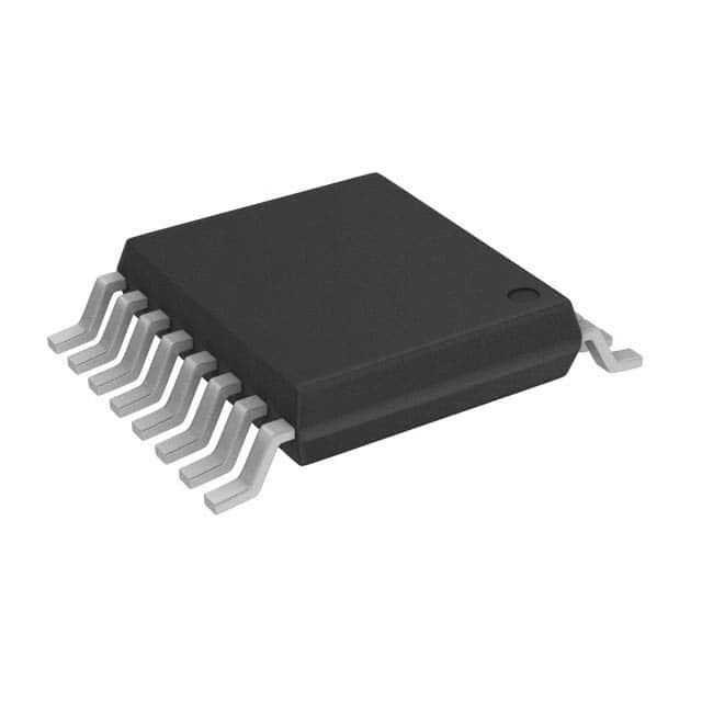
- Part No.:
- DG412DQ-T1-E3
- Manufacturer:
- Vishay Siliconix
- Package:
- 16-TSSOP (0.173", 4.40mm Width)
- Datasheet:
-
 DG412DQ-T1-E3.pdf
- Description:
- IC SW SPST-NOX4 35OHM 16TSSOP
- Quantity:
- Payment:

- Shipping:

Inventory:19,147
Please send an inquiry. Send us your inquiry, and we will respond immediately.
Product details
Overview
DG412DQ-T1-E3 from Vishay Intertechnology is a Vishay Siliconix precision monolithic quad SPST CMOS analog switch designed for high-speed, low-error switching of precision analog signals. The DG412 configuration provides four normally open SPST switches with TTL and CMOS compatible logic control, ±15 V analog signal range, 25 Ω typical on-resistance, 110 ns typical turn-on time, and ultra-low 0.35 μW power dissipation.
For engineers reviewing the DG412DQ-T1-E3 datasheet, DG412DQ-T1-E3 pinout, DG412DQ-T1-E3 application, or DG412DQ-T1-E3 equivalent, this device is most relevant for precision data acquisition, automatic test equipment, communication systems, battery-powered equipment, and analog signal routing circuits requiring four low-leakage CMOS switch channels in a 16-pin TSSOP package.
Technical Context
DG412DQ-T1-E3 uses the DG412 normally open control logic: a logic 0 keeps each switch off, while a logic 1 turns the switch on. The family supports ±15 V analog signal handling under dual-supply operation, 5 V to 44 V single-supply operation, and a 44 V maximum V+ to V- supply rating, allowing the switch array to route precision analog signals across a wide dynamic range.
The analog switch specifications include 25 Ω typical drain-source on-resistance, 0.25 nA maximum room-temperature off leakage, 0.1 nA typical on leakage, 5 pC typical charge injection, 35 pF source-on capacitance, 9 pF source-off capacitance, 68 dB off isolation, and 85 dB channel-to-channel crosstalk at 1 MHz test conditions. The -40 °C to +85 °C D-suffix temperature range supports industrial signal-routing designs.
Key Specifications
| Parameter | Value and Actual Design Meaning |
|---|---|
| Device Type | Precision monolithic quad SPST CMOS analog switch for analog signal routing and multiplexing functions. |
| Switch Configuration | Four normally open SPST switches; logic 0 = off and logic 1 = on for DG412. |
| Analog Signal Range | ±15 V under the specified dual-supply operating condition, supporting wide-range precision signal paths. |
| Supply Capability | Single-supply operation from 5 V to 44 V and dual-supply operation up to ±22 V class according to the product summary. |
| On-Resistance | 25 Ω typical RDS(on), with 35 Ω room-temperature maximum and 45 Ω full-temperature maximum under ±15 V supply test conditions. |
| Switching Speed | 110 ns typical turn-on time and 100 ns typical turn-off time, supporting fast analog path selection. |
| Leakage Performance | 0.25 nA maximum room-temperature off leakage and 0.1 nA typical on leakage for low-error precision analog switching. |
| Charge Injection | 5 pC typical charge injection, relevant to sample-and-hold, data acquisition, and high-impedance signal-chain circuits. |
| Capacitance | 35 pF source-on capacitance and 9 pF source-off capacitance at 1 MHz test conditions. |
| Logic Compatibility | TTL and CMOS compatible logic with logic 0 ≤ 0.8 V and logic 1 ≥ 2.4 V. |
| Temperature Range | -40 °C to +85 °C for the D-suffix ordering option. |
| Package | 16-pin TSSOP package identified by the DQ package code, supplied with T1 reel packaging and E3 compliant termination code. |
Pinout & Package
DG412DQ-T1-E3 is supplied in a 16-pin TSSOP package. The TSSOP-16 body provides a compact 0.65 mm pitch surface-mount footprint with 5.00 mm nominal body length and 4.40 mm nominal body width, helping engineers place four analog switch channels, dual supplies, logic supply, and ground reference in space-constrained precision signal-chain layouts.
| Pin / Terminal | Circuit Role | Design Meaning |
|---|---|---|
| IN1, IN2, IN3, IN4 | Digital control inputs for the four SPST switch channels. | Each input controls its corresponding analog switch; for DG412, logic 1 turns the channel on and logic 0 turns the channel off. |
| S1, S2, S3, S4 | Analog source terminals for the four switch channels. | Connect to one side of each bidirectional analog signal path; each switch conducts in either direction when turned on. |
| D1, D2, D3, D4 | Analog drain terminals for the four switch channels. | Connect to the opposite side of each analog path, allowing signal routing, gating, or channel selection between source and drain nodes. |
| V+ | Positive analog supply rail. | Defines the positive supply boundary for the analog switch array and supports wide-signal-range operation with the negative supply rail. |
| V- | Negative analog supply rail. | Defines the negative analog signal boundary for bipolar analog switching, including ±15 V signal-chain operation. |
| VL | Logic supply input. | Sets the logic-control supply domain for TTL and CMOS input compatibility. |
| GND | Logic ground and circuit reference. | Provides the ground reference for the control interface and must be tied to the system logic ground for correct input threshold behavior. |
Key Features
- Quad normally open SPST CMOS analog switch configuration for four independent signal paths.
- ±15 V analog signal range with 44 V maximum V+ to V- supply rating for wide dynamic range switching.
- 25 Ω typical on-resistance for low-error precision analog routing.
- 110 ns typical turn-on time and 100 ns typical turn-off time for fast channel selection.
- 5 pC typical charge injection and low leakage performance for precision data acquisition circuits.
- TTL and CMOS compatible control inputs with single-supply and dual-supply operation capability.
Applications
| Precision Data Acquisition | Automatic Test Equipment |
|---|---|
|
Use Scenario: Analog front-end systems that route sensor or measurement signals into ADC and signal-conditioning stages. IC Role: Four-channel normally open analog switch for precision signal selection. Use Value: Low leakage, 25 Ω typical on-resistance, and 5 pC charge injection help reduce switching error in measurement paths. |
Use Scenario: Test fixtures and precision ATE channels requiring repeated analog path connection and disconnection. IC Role: CMOS switch array for controlled analog routing under TTL or CMOS logic. Use Value: 110 ns typical turn-on time and quad SPST structure allow fast, compact routing of multiple test signals. |
| Communication Signal Routing | Battery-Powered Instrumentation |
|
Use Scenario: Communication equipment and interface circuits that need low-distortion analog path switching. IC Role: Bidirectional analog switch with source and drain terminals conducting equally well when on. Use Value: ±15 V analog range, 68 dB off isolation, and 85 dB channel-to-channel crosstalk performance support cleaner analog signal routing. |
Use Scenario: Portable industrial instruments and battery-powered measurement electronics. IC Role: Ultra-low-power quad analog switch for signal gating and function selection. Use Value: 0.35 μW power dissipation and single-supply capability help reduce system power budget while retaining four analog switch channels. |
Equivalent & Alternatives
When evaluating DG412DQ-T1-E3 equivalent devices, engineers should compare switch configuration, normally open or normally closed logic behavior, on-resistance, leakage current, analog signal range, supply mode, charge injection, package, and control-interface requirements.
| Alternative Part | Technical Difference | Application Difference | Selection Advice |
|---|---|---|---|
| DG411DQ-T1-E3 | Same 16-pin TSSOP package and quad SPST analog switch family, but DG411 uses normally closed switch logic instead of DG412 normally open logic. | Better suited when the default or logic-low state should connect the analog path rather than leave it open. | Select DG412DQ-T1-E3 for normally open behavior; select DG411DQ-T1-E3 when opposite control polarity is required. |
| DG413DQ-T1-E3 | Same package family with a complementary configuration: two switches follow one logic sense and two switches follow the opposite sense. | Useful for analog routing circuits that require paired or complementary signal-path control. | Choose DG413DQ-T1-E3 when the circuit needs mixed normally open and normally closed behavior in one package. |
| DG412DY-T1-E3 | Same DG412 normally open quad SPST analog switch function but supplied in 16-pin narrow SOIC rather than 16-pin TSSOP. | Better suited when the PCB layout, assembly process, or legacy footprint uses narrow SOIC packaging. | Select DG412DQ-T1-E3 for compact TSSOP placement; select DG412DY-T1-E3 when SOIC footprint compatibility is required. |
Compared with DG411DQ-T1-E3, DG412DQ-T1-E3 is optimized for normally open analog signal routing, where a logic-high command connects each switch. DG412DQ-T1-E3 vs DG413DQ-T1-E3 selection depends on switch logic architecture, while DG412DQ-T1-E3 vs DG412DY-T1-E3 selection depends mainly on TSSOP versus SOIC layout and production assembly requirements.
Quality
DG412DQ-T1-E3 should be sourced as original Vishay Intertechnology components through traceable and controlled supply channels. Quality verification procedures may include TSSOP package inspection, top-mark validation, solderability testing, control-input threshold verification, on-resistance screening, leakage-current measurement, switching-time characterization, charge-injection review, and incoming inspection according to precision analog signal-chain production requirements.
Availability
DG412DQ-T1-E3 is available at Aetrix Electronics and suitable for precision data acquisition, automatic test equipment, and low-error analog signal routing platforms requiring stable component supply and repeatable production support.
Supply support may include scheduled delivery planning, volume procurement support, BOM continuity assistance, traceable sourcing management, and long-term availability support for OEM manufacturers, industrial instrumentation developers, communication-equipment designers, and electronics production programs.
For production deployment, confirming the 16-pin TSSOP package, normally open DG412 switch logic, analog signal range, supply configuration, leakage and on-resistance requirements, lifecycle status, environmental specifications, and sourcing continuity helps reduce procurement risk and improve manufacturing stability.
Manufacturer
Vishay Intertechnology supplies Vishay Siliconix analog switch and signal-routing products for precision, industrial, communication, and portable electronics. The DG411, DG412, and DG413 family uses Vishay Siliconix CMOS switch technology to combine wide signal range, low leakage, fast switching, and low-power operation in standard surface-mount packages.
FAQ
What is DG412DQ-T1-E3 used for?
DG412DQ-T1-E3 is used for precision analog signal routing in data acquisition, automatic test equipment, communication systems, battery-powered instruments, and computer peripheral circuits requiring four normally open CMOS switch channels.
Is DG412DQ-T1-E3 normally open or normally closed?
DG412DQ-T1-E3 is normally open. For the DG412 logic table, logic 0 turns the switch off and logic 1 turns the switch on.
What package is used by DG412DQ-T1-E3?
DG412DQ-T1-E3 uses a 16-pin TSSOP package. The DQ package option provides a compact surface-mount footprint for four analog switch channels, dual analog supplies, logic supply, and control pins.
What should be considered in DG412DQ-T1-E3 pinout design?
DG412DQ-T1-E3 pinout design should keep the S1 to S4 and D1 to D4 analog paths short and symmetrical where precision matters, connect V+, V-, VL, and GND to stable supply rails, and route IN1 to IN4 from TTL or CMOS logic signals according to the normally open control behavior.
What are common DG412DQ-T1-E3 equivalent options?
Common comparison options include DG411DQ-T1-E3 for normally closed switch logic, DG413DQ-T1-E3 for complementary switch behavior, and DG412DY-T1-E3 when the same DG412 function is needed in a 16-pin narrow SOIC package.
DG412DQ-T1-E3 Specifications
- Product attributes
- Attribute value
- Manufacturer:
- Vishay Siliconix
- Series:
- -
- Packaging:
- Tape & Reel (TR)
- Product Status:
- Active
- Switch Circuit:
- SPST - NO
- Multiplexer/Demultiplexer Circuit:
- 1:1
- Number of Circuits:
- 4
- On-State Resistance (Max):
- 35Ohm
- Channel-to-Channel Matching (ΔRon):
- -
- Voltage - Supply, Single (V+):
- -
- Voltage - Supply, Dual (V±):
- ±15V
- Switch Time (Ton, Toff) (Max):
- 175ns, 145ns
- -3db Bandwidth:
- -
- Charge Injection:
- 5pC
- Channel Capacitance (CS(off), CD(off)):
- 9pF, 9pF
- Current - Leakage (IS(off)) (Max):
- 250pA
- Crosstalk:
- -85dB @ 1MHz
- Operating Temperature:
- -40°C ~ 85°C (TA)
- Grade:
- -
- Qualification:
- -
- Mounting Type:
- Surface Mount
- Supplier Device Package:
- 16-TSSOP
DG412DQ-T1-E3 FAQ
1.How can I place an order for DG412DQ-T1-E3 through Aetrix?
Please submit a Request for Quotation (RFQ) for DG412DQ-T1-E3 on Aetrix. Our sales agent will provide a competitive quotation and guide you through the order confirmation once you accept the terms.
2.Are the price and stock information for DG412DQ-T1-E3 reliable?
The price and inventory of DG412DQ-T1-E3 are updated periodically and may fluctuate due to market conditions. Stock and pricing data are typically refreshed every 24 hours. Quotation validity for DG412DQ-T1-E3 is usually 5 days.
3.What payment methods are accepted for DG412DQ-T1-E3?
We accept Wire Transfer, PayPal, Credit Card, Western Union, MoneyGram, and Escrow for DG412DQ-T1-E3 transactions.
Note: Certain payment methods may incur a processing fee.
4.How is shipping managed for DG412DQ-T1-E3?
DG412DQ-T1-E3 orders can be shipped via leading logistics carriers, including DHL, UPS, FedEx, TNT, or Registered Mail.
Once your DG412DQ-T1-E3 order is processed, you will receive an email with the shipment details and tracking number.
Note: Tracking information may take up to 24 hours to appear. Express delivery typically takes 3–5 business days.
5.How can I obtain technical support or documentation for DG412DQ-T1-E3?
For technical support, including DG412DQ-T1-E3 datasheets, pinout diagrams, or application guidance, please contact our engineering support team. They can provide detailed documentation and assistance for your DG412DQ-T1-E3 requirements.
6.How does Aetrix verify that DG412DQ-T1-E3 is sourced from the original manufacturer or authorized distributors?
All DG412DQ-T1-E3 products on Aetrix are procured from qualified distributors and authorized channels. Our dedicated quality assurance team conducts strict verification, including traceability checks and, if necessary, third-party testing. This ensures that DG412DQ-T1-E3 meets industry standards.
7.What is the process for return or replacement of DG412DQ-T1-E3?
All DG412DQ-T1-E3 units undergo pre-shipment inspection (PSI). If there is an issue with DG412DQ-T1-E3, returns or replacements are accepted under the following conditions:
1.Quantity discrepancies, incorrect items, or visible external defects (such as breakage or corrosion), acknowledged by Aetrix.
2.The issue is reported within 90 days of delivery.
3.The DG412DQ-T1-E3 part is unused and in its original packaging.
Return procedure for DG412DQ-T1-E3:
1.Submit a request within 90 days.
2.Obtain a Return Material Authorization (RMA) from Aetrix.
DG412DQ-T1-E3 Tags

-
SN74LVC1G3157DBVR
Texas Instruments

-
SN74LVC1G66DBVR
Texas Instruments

-
SN74LVC1G66DCKR
Texas Instruments
-
SN74LVC1G3157DSFR
Texas Instruments

-
1P1G3157QDCKRQ1
Texas Instruments

-
SN74LVC2G66DCUR
Texas Instruments

-
SN74LV4052APWR
Texas Instruments
-
74HC4051D,653
Nexperia USA Inc.
-
SN74LV4051APWR
Texas Instruments
-
CD74HC4052PWR
Texas Instruments
-
CD74HC4051PWR
Texas Instruments
-
TS5A3166DBVR
Texas Instruments
Tech Hub

Jumper cables guide covering safe connection order, red and black clamp placement, final ground connection, cable gauge, length, clamp quality, copper vs CCA cables, jump starter comparison and battery…

LDO regulator guide covering low dropout voltage, power dissipation, thermal design, PSRR, output noise, capacitor stability, adjustable LDO circuits, LDO vs buck converter and datasheet selection chec…

Conditional Access Module guide covering CAM meaning, CI/CI+ interface, smart card authorization, DVB security workflow, TV and set-top box compatibility, internal electronics, ESD protection, connecto…

Guide to electronic component obsolescence covering EOL risk, PCN/PDN notices, last-time buy planning, replacement options, form-fit-function validation, counterfeit risk and BOM lifecycle management.

18650 battery guide covering lithium-ion cell basics, 3.6V/3.7V voltage, 4.2V charging, mAh and Wh capacity, protected cells, chargers, BMS, series-parallel packs, holders, welding and sourcing checks.…

Hall effect sensor guide covering working principle, linear and digital sensors, Arduino circuits, current sensing, speed detection, automotive applications, A3144 examples, signal filtering and datash…

Product Change Notification guide for electronic components, covering PCN meaning, PCN vs PDN/EOL, common change types, risk levels, form-fit-function review, engineering validation, BOM control, LTB/L…

A practical guide to blend door actuators, covering HVAC function, symptoms, location, AC and heater issues, reset and calibration, replacement cost, electrical diagnosis, compatibility checks, and rep…

Engineering guide to Raspberry Pi alternatives, covering chip-level differences, Orange Pi, ROCK, Jetson, Banana Pi, NanoPi, Compute Module, Pico, GPIO, camera, HAT compatibility, and replacement risks…

Engineering guide to dynamic load response testing for high-current buck converters, covering load step setup, slew rate, Vcore undershoot, overshoot, recovery time, probe location, output capacitors a…


