
 My Inquiry
 My Account


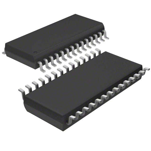
Texas Instruments DIR9001IPWRQ1
- Part No.:
- DIR9001IPWRQ1
- Manufacturer:
- Texas Instruments
- Category:
- Audio Special Purpose
- Package:
- 28-TSSOP (0.173", 4.40mm Width)
- Datasheet:
-
 DIR9001IPWRQ1.pdf
- Description:
- IC AUDIO RECEIVER 28TSSOP
- Quantity:
- Payment:

- Shipping:

Inventory:4,976
Please send an inquiry. Send us your inquiry, and we will respond immediately.
Product details
Overview
DIR9001IPWRQ1 from Texas Instruments is a 24-bit, 28–108 kHz digital audio interface receiver IC designed for automotive-grade S/PDIF and AES/EBU biphase signal decoding. It integrates low-jitter clock recovery (50 ps rms), hardware-configurable output formats (I²S, left/right-justified), and dual power supplies (2.7–3.6 V) - enabling direct integration into car audio head units and external amplifiers without external clocking.
For engineers reviewing the DIR9001IPWRQ1 datasheet, DIR9001IPWRQ1 pinout, DIR9001IPWRQ1 application, or DIR9001IPWRQ1 equivalent, this device delivers production-ready IEC60958-3/JEITA CPR-1205/AES3/EBU tech3250 compliance, selectable recovered system clocks (128fS–512fS), and 5-V-tolerant control inputs - critical for robust automotive infotainment signal integrity and layout simplicity.
Technical Context
The DIR9001IPWRQ1 implements a fully integrated PLL-based clock recovery architecture with VCO, charge pump, and external loop filter (R1=680 Ω, C1=0.068 µF, C2=0.0047 µF) to extract stable system clocks from biphase input signals. Its PLL supports lock-in across 28–108 kHz sampling frequencies and complies with IEC60958-3 jitter tolerance requirements.
It features three hardware-selectable operation modes (PLL, XTI, AUTO) via the CKSEL pin, with dedicated outputs for channel-status (COUT), user data (UOUT), pre-emphasis (EMPH), and actual sampling frequency (FSOUT0/FSOUT1). All digital I/Os except XTI are 5-V tolerant TTL, and no external clock is required for basic decode operation when XTI is grounded.
Key Specifications
| Parameter | Value and Actual Design Meaning |
|---|---|
| Biphase Input Range | 28 kHz to 108 kHz sampling frequency - covers CD (44.1 kHz), DVD (48 kHz), and high-res audio (88.2/96 kHz) standards |
| Recovered Clock Jitter | 50 ps rms (typical) - meets low-jitter requirements for high-fidelity DAC clocking in automotive audio |
| Output Clock Options | 128fS, 256fS, 384fS, 512fS - enables flexible interface to common audio DACs and DSPs |
| Data Output Formats | 24-bit I²S, 24-bit left-justified, 16/24-bit right-justified - supports legacy and modern audio subsystems |
| Supply Voltage | 2.7 V to 3.6 V (dual rail: VCC/VDD) - compatible with standard 3.3 V automotive power domains |
| Digital Input Tolerance | 5-V tolerant on RXIN, FMT0/1, PSCK0/1, CKSEL, RST, RSV - simplifies level-shifting in mixed-voltage systems |
| Operating Temperature | –40°C to +85°C - qualified for under-dash automotive environments per AEC-Q100 stress testing |
Pinout & Package
Package: 28-pin TSSOP (0.65 mm pitch), RoHS-compliant, thermal resistance θJA = 105 °C/W.
| Pin/Terminal | Circuit Role | Design Meaning |
|---|---|---|
| RXIN | Biphase serial input | 5-V tolerant TTL input for S/PDIF or AES3 signal - accepts optical (TOSLINK) or coaxial sources directly |
| SCKO | System clock output | CMOS output of recovered clock (128fS–512fS) - drives DAC master clock or FPGA reference |
| BCKO | Bit clock output | 64fS CMOS bit clock - synchronizes serial audio data transfer to downstream devices |
| LRCKO | Word clock output | fS latch-enable clock - defines left/right channel boundaries for stereo audio framing |
| DOUT | Decoded audio data | 24-bit serial audio output (I²S/left/right-justified) - feeds DAC or audio processor without buffering |
| COUT / UOUT | Channel-status / User data | Serial outputs synchronized to LRCKO - enable metadata parsing (sample rate, pre-emphasis, copy protection) |
| CKSEL | Clock source select | Hardware mode control: L = PLL recovery, H = XTI source, connected to ERROR = AUTO switching |
| RST | Active-low reset | 5-V tolerant TTL input requiring ≥100 ns pulse after VDD > 2.7 V - ensures deterministic startup state |
| FILT | PLL loop filter node | Analog connection point for external RC filter - critical for stable PLL lock and jitter performance |
Key Features
| Feature | Design Value |
|---|---|
| No external clock required for decode | XTI pin can be tied to DGND - eliminates BOM cost and board space for crystal/resonator in basic applications |
| Hardware-only configuration | All functions (format, clock selection, mode) controlled by logic-level pins - no microcontroller or firmware needed |
| Automotive temperature range | –40°C to +85°C operation - validated for head unit and amplifier mounting locations with minimal thermal margin |
| IEC60958-3 compliant jitter tolerance | Meets Level III capture ratio (±12.5%) - ensures reliable lock under real-world transmission impairments |
| Dedicated status outputs | ERROR, CLKST, BFRAME, FSOUT0/1 - provide real-time PLL lock status, block alignment, and calculated fS for diagnostics |
Applications
| Car Audio Head Units | Car Audio External Amplifiers |
|---|---|
Use Scenario: Digital audio stream from navigation system or Bluetooth module routed to head unit mainboard. IC Role / Device Role / Timing Role: Receives S/PDIF biphase signal, recovers low-jitter clock, and outputs I²S data + LRCKO/BCKO to internal DAC. Use Value: Eliminates need for separate clock generator and reduces EMI risk by avoiding high-speed clock routing across PCB. |
Use Scenario: High-power Class-D amplifier receiving digital audio from factory head unit via coaxial S/PDIF. IC Role / Device Role / Timing Role: Decodes incoming AES3/S/PDIF, provides clean 256fS system clock and 24-bit right-justified data to amplifier's audio processor. Use Value: Enables bit-perfect audio reproduction with <50 ps clock jitter - critical for THD+N < 0.005% amplifier performance. |
| Automotive Infotainment Gateways | Aftermarket DSP Processors |
Use Scenario: Central gateway aggregating digital audio from multiple sources (USB, HDMI ARC, tuner) into unified bus. IC Role / Device Role / Timing Role: Acts as standardized S/PDIF receiver front-end, feeding decoded data and channel-status bits to SoC via parallel interface. Use Value: Hardware-controlled format selection (FMT0/FMT1) allows dynamic reconfiguration between I²S and left-justified without software intervention. |
Use Scenario: Compact DSP module adding active crossover and EQ to OEM audio systems via optical input. IC Role / Device Role / Timing Role: Receives TOSLINK signal, outputs synchronized UOUT/COUT metadata and 24-bit DOUT to DSP core for real-time processing. Use Value: Direct access to pre-emphasis (EMPH), sampling frequency (FSOUT0/1), and error flags enables adaptive audio compensation algorithms. |
Equivalent & Alternatives
The following parts are listed as comparable options for similar digital audio interface receiver applications.
| Alternative Part | Technical Difference | Application Difference | Selection Advice |
|---|---|---|---|
| CS8416-CZZR | Supports up to 192 kHz, includes SPI control interface and more channel-status registers; requires external 27 MHz clock for full spec. | Preferred for professional audio gear needing extended sample rates and firmware configurability. | Choose CS8416-CZZR if SPI control, 192 kHz support, or enhanced metadata handling is required - not drop-in compatible due to different pinout and clocking. |
| AK4115VT-E2 | Offers 100 kHz max input, integrated PLL loop filter, and lower supply current (5.2 mA); lacks FSOUT outputs and AUTO mode. | Better suited for space-constrained consumer audio where simplified layout and lower power outweigh diagnostic flexibility. | Choose AK4115VT-E2 for cost-sensitive, low-power designs where sampling frequency detection and automatic clock switching are unnecessary. |
Compared with DIR9001IPWRQ1, CS8416-CZZR adds configurability at the cost of higher complexity and non-pin-compatible layout, while AK4115VT-E2 trades diagnostic capability and automotive qualification for smaller footprint and lower quiescent current - making DIR9001IPWRQ1 optimal for AEC-Q100-compliant automotive systems requiring hardware simplicity and robust status monitoring.
Availability
DIR9001IPWRQ1 is available at Aetrix Electronics and suitable for car audio head units, automotive external amplifiers, infotainment gateways, and aftermarket DSP processors requiring stable component supply across extended temperature ranges and long production lifecycles.
Supply support for DIR9001IPWRQ1 includes scheduled delivery planning, volume procurement assistance, BOM continuity management, traceable sourcing, and lifecycle availability coordination for OEM customers, industrial embedded developers, connected-device designers, and electronics production programs.
Manufacturer
Texas Instruments is a global semiconductor leader specializing in analog, embedded processing, and automotive electronics, with decades of experience in high-reliability signal chain solutions.
The DIR9001IPWRQ1 belongs to TI's automotive-qualified digital audio interface product line, engineered specifically for noise-immune, low-jitter S/PDIF and AES3 reception in harsh vehicle environments - emphasizing hardware configurability, AEC-Q100 compliance, and seamless integration with TI's C5000/C6000 DSPs and PCM codecs.
FAQ
Does DIR9001IPWRQ1 require an external crystal or resonator to operate?
No, DIR9001IPWRQ1 does not require an external crystal or resonator for basic biphase decode operation. When XTI is connected to DGND, the device uses its internal PLL to recover clock and data from the RXIN signal. An external 24.576-MHz resonator or clock is only needed for the actual-sampling-frequency calculator function or when operating in XTI mode (CKSEL = H).
What is the purpose of the FILT pin on DIR9001IPWRQ1?
The FILT pin on DIR9001IPWRQ1 connects to an external passive loop filter (R1=680 Ω, C1=0.068 µF, C2=0.0047 µF) that stabilizes the internal PLL's charge pump and VCO. This filter is mandatory in PLL mode (CKSEL = L) to ensure reliable lock acquisition, low jitter (<50 ps rms), and immunity to supply noise - improper filtering causes unlock events or increased clock phase noise.
Can DIR9001IPWRQ1 decode both S/PDIF and AES3 signals?
Yes, DIR9001IPWRQ1 decodes both S/PDIF and AES3 signals because it complies with IEC60958-3, JEITA CPR-1205, AES3, and EBU tech3250 standards - all of which define biphase-mark encoded digital audio interfaces. The device accepts the same biphase input on RXIN regardless of physical layer (optical TOSLINK, coaxial, or differential), with identical timing and jitter specifications.
How does the AUTO mode work on DIR9001IPWRQ1?
AUTO mode on DIR9001IPWRQ1 is enabled by connecting CKSEL to the ERROR pin. When ERROR = L (PLL locked), the device outputs the recovered PLL clock (SCKO/BCKO/LRCKO); when ERROR = H (PLL unlocked), it switches to the XTI source clock. This provides failover clocking during signal loss - but requires an external 24.576-MHz source on XTI to maintain output continuity during ERROR periods.
What are the voltage and logic-level requirements for DIR9001IPWRQ1's digital inputs?
DIR9001IPWRQ1's digital inputs (RXIN, FMT0/1, PSCK0/1, CKSEL, RST, RSV) are 5-V tolerant TTL with Schmitt-trigger inputs and internal pulldowns (except RST, which has internal pullup). VIH = 2 V min, VIL = 0.8 V max. XTI is not 5-V tolerant and must be driven at CMOS levels (0–VCC) - exceeding VCC+0.3 V risks damage.
DIR9001IPWRQ1 Specifications
- Product attributes
- Attribute value
- Manufacturer:
- Texas Instruments
- Series:
- -
- Package/Case:
- 28-TSSOP (0.173", 4.40mm Width)
- Packaging:
- Tape & Reel (TR)
- Product Status:
- Active
- Function:
- Audio Receiver
- Applications:
- Audio, Musical Instruments
- Number of Channels:
- 1
- Interface:
- I2S
- Voltage - Supply:
- 2.7V ~ 3.6V
- Operating Temperature:
- -40°C ~ 85°C (TA)
- Specifications:
- 28kHz ~ 108kHz
- Mounting Type:
- Surface Mount
- Grade:
- Automotive
DIR9001IPWRQ1 FAQ
1.How can I place an order for DIR9001IPWRQ1 through Aetrix?
Please submit a Request for Quotation (RFQ) for DIR9001IPWRQ1 on Aetrix. Our sales agent will provide a competitive quotation and guide you through the order confirmation once you accept the terms.
2.Are the price and stock information for DIR9001IPWRQ1 reliable?
The price and inventory of DIR9001IPWRQ1 are updated periodically and may fluctuate due to market conditions. Stock and pricing data are typically refreshed every 24 hours. Quotation validity for DIR9001IPWRQ1 is usually 5 days.
3.What payment methods are accepted for DIR9001IPWRQ1?
We accept Wire Transfer, PayPal, Credit Card, Western Union, MoneyGram, and Escrow for DIR9001IPWRQ1 transactions.
Note: Certain payment methods may incur a processing fee.
4.How is shipping managed for DIR9001IPWRQ1?
DIR9001IPWRQ1 orders can be shipped via leading logistics carriers, including DHL, UPS, FedEx, TNT, or Registered Mail.
Once your DIR9001IPWRQ1 order is processed, you will receive an email with the shipment details and tracking number.
Note: Tracking information may take up to 24 hours to appear. Express delivery typically takes 3–5 business days.
5.How can I obtain technical support or documentation for DIR9001IPWRQ1?
For technical support, including DIR9001IPWRQ1 datasheets, pinout diagrams, or application guidance, please contact our engineering support team. They can provide detailed documentation and assistance for your DIR9001IPWRQ1 requirements.
6.How does Aetrix verify that DIR9001IPWRQ1 is sourced from the original manufacturer or authorized distributors?
All DIR9001IPWRQ1 products on Aetrix are procured from qualified distributors and authorized channels. Our dedicated quality assurance team conducts strict verification, including traceability checks and, if necessary, third-party testing. This ensures that DIR9001IPWRQ1 meets industry standards.
7.What is the process for return or replacement of DIR9001IPWRQ1?
All DIR9001IPWRQ1 units undergo pre-shipment inspection (PSI). If there is an issue with DIR9001IPWRQ1, returns or replacements are accepted under the following conditions:
1.Quantity discrepancies, incorrect items, or visible external defects (such as breakage or corrosion), acknowledged by Aetrix.
2.The issue is reported within 90 days of delivery.
3.The DIR9001IPWRQ1 part is unused and in its original packaging.
Return procedure for DIR9001IPWRQ1:
1.Submit a request within 90 days.
2.Obtain a Return Material Authorization (RMA) from Aetrix.
DIR9001IPWRQ1 Tags

-
SA571DR2G
onsemi
-
ADAU7002ACBZ-R7
Analog Devices Inc.

-
DRV135UA/2K5
Texas Instruments

-
DRV134UA/1K
Texas Instruments

-
DRV134PA
Texas Instruments
-
DRV134UA
Texas Instruments
-
DRV135UA
Texas Instruments
-
SA572DR2G
onsemi
-
PGA2311U/1K
Texas Instruments
-
SI8244BB-D-IS1R
Skyworks Solutions Inc.

-
CS8416K-CZZR
Cirrus Logic Inc.
-
SRC4392IPFBR
Texas Instruments
Tech Hub

A practical engineering guide to 3.3V and 5V logic compatibility, input thresholds, resistor dividers, translator ICs, MOSFET level shifting, I2C pull-ups, timing limits and power-sequencing risks.

The 74HC595 uses push-pull logic outputs, while the TPIC6B595 uses 50 V open-drain DMOS sinks for higher-power loads. This guide compares timing, current limits, 3.3 V interfacing, load wiring, thermal…

The 74HC595 converts serial data into eight stable parallel outputs. This guide covers pin functions, shift and storage timing, OE and MR behavior, drive-current limits, cascading, voltage compatibilit…

A technical comparison of level-sensitive latches and edge-triggered flip-flops, covering timing windows, setup and hold limits, master–slave operation, time borrowing, race-through, HDL inference and…

A D latch stores one bit while Enable controls when data can pass. This reference covers gate-level operation, truth tables, transparency, setup and hold timing, LE versus OE, common ICs and practical …

An SR latch stores one bit through cross-coupled feedback. This engineering reference covers NOR and NAND implementations, truth tables, forbidden-state recovery, gated operation, switch debouncing, fa…

Latch circuits retain one bit through feedback. This technical reference covers SR and D latches, truth tables, transparency, timing limits, latch-versus-flip-flop behavior, applications and common log…

An engineering guide to LED driver operation, constant-current and constant-voltage outputs, linear and switching topologies, dimming, IC selection, calculations, replacement compatibility, and fault c…

Operational amplifier guide covering op amp basics, feedback, ideal vs real op amps, common configurations, buffer circuits, offset, bias current, gain-bandwidth, slew rate, rail-to-rail limits and sel…

Jumper cables guide covering safe connection order, red and black clamp placement, final ground connection, cable gauge, length, clamp quality, copper vs CCA cables, jump starter comparison and battery…


