
 My Inquiry
 My Account


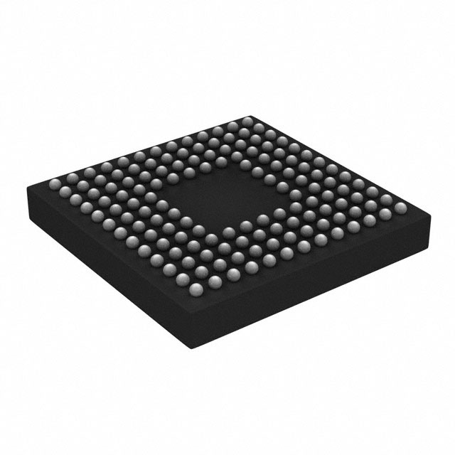
Texas Instruments DLPC3433CZVB
- Part No.:
- DLPC3433CZVB
- Manufacturer:
- Texas Instruments
- Category:
- Display Drivers
- Package:
- 176-VFBGA
- Datasheet:
-
 DLPC3433CZVB.pdf
- Description:
- IC DRVR CTLR 176NFBGA
- Quantity:
- Payment:

- Shipping:

Inventory:2,843
Please send an inquiry. Send us your inquiry, and we will respond immediately.
Product details
Overview
DLPC3433CZVB from Texas Instruments is a digital display controller IC designed specifically for the DLP3010 (.3" 720p) digital micromirror device (DMD), supporting up to 720p resolution at input frame rates up to 120 Hz, with MIPI DSI Type 3 interface (1–4 lanes, up to 470 Mbps/lane), embedded eDRAM frame memory, and IntelliBright™ image processing suite - deployed in mobile projectors and smart displays.
For engineers reviewing the DLPC3433CZVB datasheet, DLPC3433CZVB pinout, DLPC3433CZVB application, or DLPC3433CZVB equivalent, key selection criteria include DSI lane support, sub-LVDS DMD interface timing compliance, parallel/BT656 input flexibility, 155 MHz pixel clock capability, and compatibility with DLPA2000/DLPA3005 PMICs for illumination control.
Technical Context
The DLPC3433CZVB implements a dedicated video pipeline with field-scaled de-interlacing, 4:2:2 to 4:4:4 chroma interpolation, programmable degamma, and color space conversion - all executed in real time with one-frame latency. Its DMD interface uses dual-mode sub-LVDS signaling (high-speed data + low-speed control) and supports auto DMD parking via PARKZ.
It integrates a system-level I²C configuration interface, SPI flash boot support (up to 128 Mb), GPIO-controlled LED current (LED_SEL_0/1), and programmable splash screens. The controller requires external PLL reference clock (24–27 MHz) and operates with multiple power domains: VDD (1.1 V), VDDLP12 (1.2 V), VCC (3.3 V), VCC_INTF (1.8 V), and VCC_FLSH (1.8 V).
Key Specifications
| Parameter | Value and Actual Design Meaning |
|---|---|
| Max Input Resolution | 1280 × 720 (720p) - supports full HD-ready imaging without external scaling. |
| Input Frame Rate | Up to 120 Hz - enables high-refresh-rate operation for motion-sensitive applications like AR glasses. |
| Pixel Clock | Up to 155 MHz - accommodates 720p@120 Hz with BT656 or parallel interface timing margins. |
| MIPI DSI Support | Type 3, 1–4 lanes, 470 Mbps/lane - only on DLPC3433 (not DLPC3438); enables compact mobile SoC integration. |
| DMD Interface | Sub-LVDS high-speed + low-speed control - ensures reliable DLP3010 mirror actuation with <20 ms park time. |
| Embedded Memory | eDRAM frame buffer - eliminates need for external SDRAM, reducing BOM and layout complexity. |
| Power Domains | 7 independent supplies (VDD, VDDLP12, VCC, VCC_INTF, VCC_FLSH, VSS_PLLM, VSS_PLLD) - enables fine-grained power gating. |
Pinout & Package
NFBGA-176 package, 7.00 × 7.00 mm body size, 0.5 mm pitch - compatible with standard fine-pitch PCB assembly processes and thermal vias under die.
| Pin/Terminal | Circuit Role | Design Meaning |
|---|---|---|
| PARKZ (C13) | DMD fast park control | Active-low hysteresis input; asserts rapid DMD mirror parking during imminent power loss - critical for DMD lifetime preservation. |
| RESETZ (C11) | Power-on reset | Active-low hysteresis input; initiates self-configuration only after all power rails and clocks are stable. |
| DMD_HS_WDATAx_P/N (A1–A10, B1–B10) | DMD high-speed pixel data | Differential sub-LVDS pairs driving DLP3010 mirror array - require matched trace length (<±1.0") and controlled impedance (100 Ω diff). |
| DMD_HS_CLK_P/N (A5, B5) | DMD high-speed clock | Differential sub-LVDS clock synchronized to pixel data - defines DMD update timing; must meet tskew ≤ 50 ps. |
| VCC_INTF (M11, M15, N10) | I/O interface supply | 1.8 V supply for I²C, SPI, GPIO, and DSI logic - must be decoupled locally to avoid noise coupling into timing-critical interfaces. |
| HOST_IRQ (N9) | Host interrupt output | Open-drain active-low signal indicating DMD ready state or error condition - used to coordinate host processor handshaking. |
Key Features
| Feature | Design Value |
|---|---|
| IntelliBright™ image processing | Real-time local area brightness boost + content-adaptive illumination control - improves perceived contrast without increasing LED power. |
| 1D Keystone correction | Hardware-accelerated trapezoidal distortion correction - enables projector placement flexibility without GPU load. |
| Programmable degamma & color space conversion | Configurable LUT-based gamma and RGB/YUV/RGBW mapping - ensures accurate color reproduction across display panels. |
| One-frame latency | End-to-end video pipeline delay ≤ 16.7 ms at 60 Hz - essential for interactive AR and gaming applications. |
| Auto DMD parking at power down | Hardware-triggered mirror reset sequence initiated by PARKZ - prevents mechanical stress and extends DMD operational life. |
Applications
| Mobile Projector | Smart Display |
|---|---|
Use Scenario: Portable pico projector integrated into smartphones or standalone battery-powered units. IC Role / Device Role / Timing Role: Primary display controller managing DLP3010 DMD, MIPI DSI input from AP, and LED current via DLPA3005. Use Value: Enables 720p@60 Hz projection with <100 mW system power draw using embedded eDRAM and low-power DMD interface training. |
Use Scenario: Compact industrial HMI or retail kiosk with embedded DLP-based optical engine. IC Role / Device Role / Timing Role: Video interface bridge converting parallel/BT656 signals to DMD-compatible sub-LVDS timing with programmable rotation and splash screen. Use Value: Eliminates external frame buffer and reduces PCB layer count via integrated eDRAM and single-chip timing control. |
| Augmented Reality Glasses | Mobile Smart TV |
Use Scenario: Near-eye display subsystem requiring ultra-low latency and precise keystone correction for see-through optics. IC Role / Device Role / Timing Role: Real-time video processor performing 1D keystone, de-interlacing, and color coordinate adjustment before DMD drive. Use Value: Achieves ≤16.7 ms end-to-end latency and sub-pixel geometric correction - critical for minimizing motion sickness in AR. |
Use Scenario: Secondary display mode in tablets or foldables using DLP3010 as auxiliary HD panel. IC Role / Device Role / Timing Role: MIPI DSI sink controller receiving video from main SoC, applying IntelliBright™ enhancement, and driving DMD via sub-LVDS. Use Value: Leverages DSI bandwidth efficiency and TI's validated optical module ecosystem for rapid bring-up. |
Equivalent & Alternatives
The following parts are listed as comparable options for similar display controller applications.
| Alternative Part | Technical Difference | Application Difference | Selection Advice |
|---|---|---|---|
| DLPC3438CZEB | 201-pin NFBGA (13 × 13 mm); no MIPI DSI support; higher pin count for expanded GPIO and parallel interface options. | Targeted at industrial displays requiring larger parallel bus width or additional control signals - not suitable for space-constrained DSI-based mobile designs. | Select DLPC3438CZEB only when DSI is unnecessary and board area allows larger package; DLPC3433CZVB remains optimal for mobile DSI integration. |
| DLPC3478CZVB | Successor IC supporting DLP3310 (.33" 1080p); adds HDMI RX, enhanced DSI (Type 4), and larger eDRAM - not pin-compatible. | Enables 1080p resolution and HDMI-native input; requires full redesign due to different power sequencing, pinout, and firmware architecture. | DLPC3478CZVB is a next-generation upgrade path - not a drop-in replacement; DLPC3433CZVB remains preferred for cost-optimized 720p DLP3010 systems. |
Compared with DLPC3438CZEB and DLPC3478CZVB, the DLPC3433CZVB uniquely balances MIPI DSI integration, 720p performance, and 7 mm × 7 mm footprint - making it the only production-qualified option for compact, battery-powered DLP3010 projectors requiring DSI connectivity.
Availability
DLPC3433CZVB is available at Aetrix Electronics and suitable for mobile projector, augmented reality glasses, and smart display applications requiring stable component supply, long-term lifecycle support, and TI-validated optical module compatibility.
Supply support for DLPC3433CZVB includes scheduled delivery planning, volume procurement assistance, BOM continuity management, traceable sourcing, and lifecycle availability coordination for OEM customers, industrial embedded developers, connected-device designers, and electronics production programs.
Manufacturer
Texas Instruments is a global semiconductor company specializing in analog, embedded processing, and digital light processing technologies, with over 90 years of innovation in power management and signal chain solutions.
The DLPC3433CZVB belongs to TI's DLP® Pico™ display controller product line, engineered specifically for ultra-compact, low-power projection systems using DLP3010 DMD - targeting portable consumer and industrial near-eye applications.
FAQ
What is the primary function of the DLPC3433CZVB in a DLP3010-based system?
The DLPC3433CZVB serves as the dedicated digital display controller for the DLP3010 (.3" 720p) DMD, handling video input processing (including IntelliBright™ algorithms), DMD interface timing generation (sub-LVDS), and system-level control (I²C, GPIO, flash boot). It is not a general-purpose MCU but a purpose-built ASIC optimized for DLP optical engine integration. The DLPC3433CZVB enables full 720p operation with one-frame latency and hardware-accelerated keystone correction.
Does the DLPC3433CZVB support MIPI DSI, and what are the lane limitations?
Yes, the DLPC3433CZVB supports MIPI DSI Type 3 with configurable 1–4 data lanes operating up to 470 Mbps per lane - a feature exclusive to the DLPC3433 family (not available on DLPC3438). This allows direct connection to mobile application processors while maintaining bandwidth for 720p@120 Hz. The DLPC3433CZVB requires proper DSI initialization per TI's programmers guide and LP-mode entry during vertical blanking intervals.
What power supply rails does the DLPC3433CZVB require, and how are they used?
The DLPC3433CZVB requires seven distinct power domains: VDD (1.1 V core), VDDLP12 (1.2 V low-power logic), VCC (3.3 V I/O), VCC_INTF (1.8 V interface), VCC_FLSH (1.8 V SPI flash), VSS_PLLM (PLL analog ground), and VSS_PLLD (PLL digital ground). Each rail powers specific functional blocks - for example, VCC_INTF supplies I²C, SPI, and GPIO logic, while VDDLP12 drives DSI receiver circuitry. Proper sequencing (VCC first, then VDD/VDDLP12, then VCC_INTF/VCC_FLSH) is mandatory per TI's power-up guidelines.
How does the PARKZ pin function, and why is it critical for DMD reliability?
The PARKZ pin (C13) is an active-low hysteresis input that triggers fast DMD mirror parking when imminent power loss is detected - typically driven by the DLPA3005's interrupt output. Asserting PARKZ initiates a hardware-controlled sequence that resets all mirrors to a safe neutral position within 20 ms, preventing mechanical stress and electrostatic damage during uncontrolled shutdown. The DLPC3433CZVB's PARKZ implementation is validated for DLP3010 lifetime extension and must be connected per TI's recommended RC network for noise immunity.
Can the DLPC3433CZVB operate without external flash memory?
No - the DLPC3433CZVB requires external SPI flash (up to 128 Mb) for firmware storage and boot code execution; it lacks internal non-volatile program memory. During power-up, the DLPC3433CZVB loads configuration and display firmware from the connected flash device via its dedicated SPI0 interface (SPI0_CLK, SPI0_DIN, SPI0_DOUT, SPI0_CSZ0/1). Operation without flash results in failed initialization and no video output - the DLPC3433CZVB will not enter functional mode.
DLPC3433CZVB Specifications
- Product attributes
- Attribute value
- Manufacturer:
- Texas Instruments
- Series:
- -
- Package/Case:
- 176-VFBGA
- Packaging:
- Tray
- Product Status:
- Active
- Display Type:
- DLP
- Configuration:
- -
- Interface:
- I2C
- Digits or Characters:
- -
- Current - Supply:
- -
- Voltage - Supply:
- 1.1V
- Operating Temperature:
- -30°C ~ 85°C
- Grade:
- -
- Qualification:
- -
- Mounting Type:
- Surface Mount
- Supplier Device Package:
- 176-NFBGA (7x7)
DLPC3433CZVB FAQ
1.How can I place an order for DLPC3433CZVB through Aetrix?
Please submit a Request for Quotation (RFQ) for DLPC3433CZVB on Aetrix. Our sales agent will provide a competitive quotation and guide you through the order confirmation once you accept the terms.
2.Are the price and stock information for DLPC3433CZVB reliable?
The price and inventory of DLPC3433CZVB are updated periodically and may fluctuate due to market conditions. Stock and pricing data are typically refreshed every 24 hours. Quotation validity for DLPC3433CZVB is usually 5 days.
3.What payment methods are accepted for DLPC3433CZVB?
We accept Wire Transfer, PayPal, Credit Card, Western Union, MoneyGram, and Escrow for DLPC3433CZVB transactions.
Note: Certain payment methods may incur a processing fee.
4.How is shipping managed for DLPC3433CZVB?
DLPC3433CZVB orders can be shipped via leading logistics carriers, including DHL, UPS, FedEx, TNT, or Registered Mail.
Once your DLPC3433CZVB order is processed, you will receive an email with the shipment details and tracking number.
Note: Tracking information may take up to 24 hours to appear. Express delivery typically takes 3–5 business days.
5.How can I obtain technical support or documentation for DLPC3433CZVB?
For technical support, including DLPC3433CZVB datasheets, pinout diagrams, or application guidance, please contact our engineering support team. They can provide detailed documentation and assistance for your DLPC3433CZVB requirements.
6.How does Aetrix verify that DLPC3433CZVB is sourced from the original manufacturer or authorized distributors?
All DLPC3433CZVB products on Aetrix are procured from qualified distributors and authorized channels. Our dedicated quality assurance team conducts strict verification, including traceability checks and, if necessary, third-party testing. This ensures that DLPC3433CZVB meets industry standards.
7.What is the process for return or replacement of DLPC3433CZVB?
All DLPC3433CZVB units undergo pre-shipment inspection (PSI). If there is an issue with DLPC3433CZVB, returns or replacements are accepted under the following conditions:
1.Quantity discrepancies, incorrect items, or visible external defects (such as breakage or corrosion), acknowledged by Aetrix.
2.The issue is reported within 90 days of delivery.
3.The DLPC3433CZVB part is unused and in its original packaging.
Return procedure for DLPC3433CZVB:
1.Submit a request within 90 days.
2.Obtain a Return Material Authorization (RMA) from Aetrix.
DLPC3433CZVB Tags
-
PCA8561AHN/AY
NXP Semiconductors

-
SN74LS47N
Texas Instruments

-
PCF85176T/1Y
NXP Semiconductors
-
PCF85176H/1,518
NXP Semiconductors
-
BU9796AMUV-E2
Rohm Semiconductor
-
PCA85176H/Q900/1,5
NXP Semiconductors
-
PCF8537AH/1,518
NXP Semiconductors
-
LM3914VX/NOPB
Texas Instruments

-
PCF85134HL/1,118
NXP Semiconductors
-
AS1115-BSST
ams-OSRAM USA INC.
-
PCA8534AH/Q900/1,5
NXP Semiconductors
-
LM3914V/NOPB
Texas Instruments
Tech Hub

A practical engineering guide to 3.3V and 5V logic compatibility, input thresholds, resistor dividers, translator ICs, MOSFET level shifting, I2C pull-ups, timing limits and power-sequencing risks.

The 74HC595 uses push-pull logic outputs, while the TPIC6B595 uses 50 V open-drain DMOS sinks for higher-power loads. This guide compares timing, current limits, 3.3 V interfacing, load wiring, thermal…

The 74HC595 converts serial data into eight stable parallel outputs. This guide covers pin functions, shift and storage timing, OE and MR behavior, drive-current limits, cascading, voltage compatibilit…

A technical comparison of level-sensitive latches and edge-triggered flip-flops, covering timing windows, setup and hold limits, master–slave operation, time borrowing, race-through, HDL inference and…

A D latch stores one bit while Enable controls when data can pass. This reference covers gate-level operation, truth tables, transparency, setup and hold timing, LE versus OE, common ICs and practical …

An SR latch stores one bit through cross-coupled feedback. This engineering reference covers NOR and NAND implementations, truth tables, forbidden-state recovery, gated operation, switch debouncing, fa…

Latch circuits retain one bit through feedback. This technical reference covers SR and D latches, truth tables, transparency, timing limits, latch-versus-flip-flop behavior, applications and common log…

An engineering guide to LED driver operation, constant-current and constant-voltage outputs, linear and switching topologies, dimming, IC selection, calculations, replacement compatibility, and fault c…

Operational amplifier guide covering op amp basics, feedback, ideal vs real op amps, common configurations, buffer circuits, offset, bias current, gain-bandwidth, slew rate, rail-to-rail limits and sel…

Jumper cables guide covering safe connection order, red and black clamp placement, final ground connection, cable gauge, length, clamp quality, copper vs CCA cables, jump starter comparison and battery…


