
 My Inquiry
 My Account


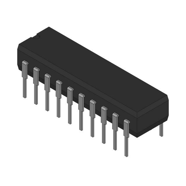
onsemi DM74ALS374N
- Part No.:
- DM74ALS374N
- Manufacturer:
- onsemi
- Category:
- Flip Flops
- Package:
- 20-DIP (0.300", 7.62mm)
- Datasheet:
-
 DM74ALS374N.pdf
- Description:
- IC FF D-TYPE SNGL 8BIT 20DIP
- Quantity:
- Payment:

- Shipping:

Inventory:2,595
Please send an inquiry. Send us your inquiry, and we will respond immediately.
Product details
Overview
DM74ALS374N from Fairchild Semiconductor is an octal 3-STATE D-type edge-triggered flip-flop in a 20-lead PDIP package, operating at 5 V with 35 MHz max clock frequency, 10 ns data setup time, and ±24 mA output drive capability. It serves as a bus-oriented register for I/O port buffering and bidirectional data latching in TTL-compatible digital systems.
For engineers reviewing the DM74ALS374N datasheet, pinout, applications, or equivalent options, key selection criteria include positive-edge clock triggering, independent 3-STATE output control, guaranteed AC performance over 0°C to +70°C, and compatibility with LS TTL logic families in bus-holding configurations.
Technical Context
The DM74ALS374N implements eight independent D-type flip-flops, each triggered on the positive edge of the clock input (CLK), with synchronous data capture from D0–D7 to Q0–Q7. Its output enable (OE) signal operates asynchronously to place all eight outputs into high-impedance state without affecting internal latch states.
This device uses advanced oxide-isolated, ion-implanted Schottky TTL process, delivering improved AC performance versus DM74LS374 while consuming approximately half the power. It guarantees switching specifications at 50 pF load across full temperature and VCC range (4.5 V to 5.5 V).
Key Specifications
| Parameter | Value and Actual Design Meaning |
|---|---|
| Logic Family | Advanced Low-Power Schottky (ALS) TTL - ensures compatibility with LS TTL and lower power than standard TTL |
| Max Clock Frequency | 35 MHz - supports high-speed bus interface timing in legacy computing and industrial control systems |
| Data Setup Time | 10 ns - defines minimum D-input stability window before CLK rising edge for reliable latching |
| Output Drive | −2.6 mA (IOH), 24 mA (IOL) - enables direct driving of capacitive bus lines without external buffers |
| Propagation Delay | 3–16 ns (tPLH/tPHL) - determines worst-case path delay between CLK edge and valid Q output transition |
| Operating Temperature | 0°C to +70°C - specifies commercial-grade ambient range for stable operation in non-extended environments |
| Supply Voltage | 4.5 V to 5.5 V - defines allowable VCC tolerance for robust noise margin and logic level integrity |
Pinout & Package
DM74ALS374N is housed in a 20-lead Plastic Dual-In-Line Package (PDIP), JEDEC MS-001 compliant, 0.300-inch wide body with 0.100-inch lead pitch. Thermal resistance θJA is 60.0°C/W.
| Pin/Terminal | Circuit Role | Design Meaning |
|---|---|---|
| 1 (OE) | Output Enable | Active-low control: drives all Q outputs to high-impedance when LOW; no effect on internal flip-flop state |
| 2–9 (D0–D7) | Data Inputs | Synchronous parallel data inputs sampled on CLK rising edge |
| 10 (GND) | Ground | Reference return path for all logic and output currents |
| 11–18 (Q0–Q7) | Registered Outputs | 3-STATE latched outputs reflecting D-input values captured at last CLK rising edge |
| 19 (CLK) | Clock Input | Positive-edge-triggered master clock controlling simultaneous data capture across all eight bits |
| 20 (VCC) | Power Supply | +5 V supply rail supporting ALS TTL voltage and current requirements |
Key Features
| Feature | Design Value |
|---|---|
| Edge-triggered D-type latches | Eight independent flip-flops synchronized to CLK rising edge - eliminates metastability risk in synchronous bus transfers |
| Asynchronous 3-STATE output control | OE pin disables outputs without altering stored data - enables multi-master bus arbitration and hot-swap safe I/O isolation |
| Bus-driver optimized outputs | Totem-pole outputs with ±24 mA drive - directly interfaces with high-capacitance backplanes and legacy TTL loads |
| LS TTL pin-for-pin compatibility | Matches DM74LS374 footprint and signal mapping - allows drop-in upgrade path with 50% power reduction |
| Guaranteed AC specs at 50 pF | Timing parameters validated under standardized capacitive loading - ensures predictable timing closure in PCB-level designs |
Applications
| Industrial PLC I/O Module | Legacy Computer Bus Interface |
|---|---|
Use Scenario: Isolating and latching sensor/actuator signals in programmable logic controller racks with shared backplane data buses. IC Role / Device Role / Timing Role: Acts as an 8-bit input register capturing parallel field data on CLK edge, then presenting it to CPU via 3-STATE outputs controlled by OE. Use Value: Enables deterministic sampling of real-time I/O with zero hold-time requirement (tH = 0 ns) and bus contention avoidance during read cycles. | Use Scenario: Buffering address/data lines between CPU and peripheral cards in ISA or Multibus-based systems. IC Role / Device Role / Timing Role: Functions as bidirectional bus transceiver register - latching outbound data on write, presenting inbound data on read via OE-controlled directionality. Use Value: Eliminates need for discrete pull-up resistors or interface logic due to totem-pole 3-STATE outputs capable of driving 50 pF loads directly. |
| Test Equipment Digital Pattern Generator | Automated Test Fixture Control |
Use Scenario: Generating precise, synchronized digital stimulus waveforms for IC functional testing using pattern memory and clock sequencing. IC Role / Device Role / Timing Role: Stores test vector bits from pattern RAM and releases them synchronously onto output pins under CLK and OE control. Use Value: Provides sub-10 ns setup margin and 3–16 ns propagation delay consistency - critical for generating glitch-free, timing-accurate stimulus edges. | Use Scenario: Controlling relay banks, LED indicators, and solenoid drivers in manufacturing test jigs requiring isolated, noise-immune digital outputs. IC Role / Device Role / Timing Role: Serves as an output latch holding steady-state control signals while allowing CPU to refresh other registers or execute instructions. Use Value: Maintains output state during OE deassertion (high-Z), preventing transient glitches during system reconfiguration or interrupt servicing. |
Equivalent & Alternatives
The following parts are listed as comparable options for similar octal D-type 3-STATE register applications.
| Alternative Part | Technical Difference | Application Difference | Selection Advice |
|---|---|---|---|
| SN74ALS374N | Same ALS TTL process, identical pinout and DC/AC specs per TI datasheet; minor packaging branding variance | No functional difference - interchangeable in all legacy designs using DM74ALS374N | Select when sourcing from Texas Instruments distribution channels or requiring TI-specific traceability |
| DM74LS374N | Lower speed (25 MHz max), higher power (ICC ≈ 35 mA vs. 19 mA), same pinout and logic function | Acceptable where timing margin exists but ALS-level power savings are not required | Choose for cost-sensitive replacements where 35 MHz performance is unnecessary and legacy LS stock is available |
Compared with SN74ALS374N, DM74ALS374N offers identical functionality and timing; versus DM74LS374N, it delivers 40% higher clock rate and ~45% lower active current - making it optimal for power-constrained or speed-critical bus register roles.
Availability
DM74ALS374N is available at Aetrix Electronics and suitable for industrial PLC I/O modules, legacy computer bus interfaces, and automated test fixture control requiring stable component supply and long-term obsolescence management.
Supply support for DM74ALS374N includes scheduled delivery planning, volume procurement assistance, BOM continuity management, traceable sourcing, and lifecycle availability coordination for OEM customers, industrial embedded developers, connected-device designers, and electronics production programs.
Manufacturer
Fairchild Semiconductor was a U.S.-based semiconductor company specializing in analog and mixed-signal ICs, power management, and logic devices before its acquisition by ON Semiconductor in 2016.
The DM74ALS374N belongs to Fairchild's ALS TTL logic family, designed specifically for high-speed, low-power bus interface and data latching in industrial and computing systems requiring LS TTL compatibility.
FAQ
What is the maximum clock frequency supported by the DM74ALS374N?
The DM74ALS374N supports a maximum clock frequency of 35 MHz under recommended operating conditions (VCC = 4.5 V to 5.5 V, TA = 0°C to +70°C). This value is guaranteed across temperature and voltage ranges with 50 pF capacitive load, enabling reliable use in high-speed bus synchronization applications where timing margins are tight.
Does the DM74ALS374N require external pull-up resistors on its outputs?
No, the DM74ALS374N does not require external pull-up resistors. Its totem-pole 3-STATE outputs provide active HIGH and LOW drive capability (±24 mA), allowing direct connection to bus lines without interface components. This design eliminates bus contention and simplifies PCB layout in systems like industrial backplanes and legacy computer architectures.
Is the DM74ALS374N pin-compatible with the DM74LS374N?
Yes, the DM74ALS374N is functionally and pin-for-pin compatible with the DM74LS374N as confirmed in the Fairchild datasheet. Both share identical pin assignments, logic behavior, and package outlines (e.g., N20A PDIP), enabling direct replacement where higher speed (35 MHz vs. 25 MHz) and lower power consumption are beneficial.
What is the data hold time specification for the DM74ALS374N?
The DM74ALS374N has a data hold time (tH) of 0 ns, meaning D-inputs may change immediately after the CLK rising edge without affecting the latched output. This zero hold-time requirement simplifies timing design in synchronous systems and reduces constraints on data path routing in dense digital boards.
Can the DM74ALS374N operate outside the 0°C to +70°C temperature range?
No, the DM74ALS374N is specified only for 0°C to +70°C free-air operating temperature. While absolute maximum ratings extend to −65°C to +150°C for storage, electrical characteristics including propagation delay, setup time, and output drive are not guaranteed outside the recommended range. For extended temperature applications, consider automotive-qualified alternatives or derating analysis.
DM74ALS374N Specifications
- Product attributes
- Attribute value
- Manufacturer:
- onsemi
- Series:
- 74ALS
- Package/Case:
- 20-DIP (0.300", 7.62mm)
- Packaging:
- Tube
- Product Status:
- Obsolete
- Function:
- Standard
- Type:
- D-Type
- Output Type:
- Tri-State, Non-Inverted
- Number of Elements:
- 1
- Number of Bits per Element:
- 8
- Clock Frequency:
- 35 MHz
- Max Propagation Delay @ V, Max CL:
- 16ns @ 5V, 50pF
- Trigger Type:
- Positive Edge
- Current - Output High, Low:
- 2.6mA, 24mA
- Voltage - Supply:
- 4.5V ~ 5.5V
- Current - Quiescent (Iq):
- 19 mA
- Input Capacitance:
- -
- Operating Temperature:
- 0°C ~ 70°C (TA)
- Grade:
- -
- Qualification:
- -
- Mounting Type:
- Through Hole
- Supplier Device Package:
- 20-PDIP
DM74ALS374N FAQ
1.How can I place an order for DM74ALS374N through Aetrix?
Please submit a Request for Quotation (RFQ) for DM74ALS374N on Aetrix. Our sales agent will provide a competitive quotation and guide you through the order confirmation once you accept the terms.
2.Are the price and stock information for DM74ALS374N reliable?
The price and inventory of DM74ALS374N are updated periodically and may fluctuate due to market conditions. Stock and pricing data are typically refreshed every 24 hours. Quotation validity for DM74ALS374N is usually 5 days.
3.What payment methods are accepted for DM74ALS374N?
We accept Wire Transfer, PayPal, Credit Card, Western Union, MoneyGram, and Escrow for DM74ALS374N transactions.
Note: Certain payment methods may incur a processing fee.
4.How is shipping managed for DM74ALS374N?
DM74ALS374N orders can be shipped via leading logistics carriers, including DHL, UPS, FedEx, TNT, or Registered Mail.
Once your DM74ALS374N order is processed, you will receive an email with the shipment details and tracking number.
Note: Tracking information may take up to 24 hours to appear. Express delivery typically takes 3–5 business days.
5.How can I obtain technical support or documentation for DM74ALS374N?
For technical support, including DM74ALS374N datasheets, pinout diagrams, or application guidance, please contact our engineering support team. They can provide detailed documentation and assistance for your DM74ALS374N requirements.
6.How does Aetrix verify that DM74ALS374N is sourced from the original manufacturer or authorized distributors?
All DM74ALS374N products on Aetrix are procured from qualified distributors and authorized channels. Our dedicated quality assurance team conducts strict verification, including traceability checks and, if necessary, third-party testing. This ensures that DM74ALS374N meets industry standards.
7.What is the process for return or replacement of DM74ALS374N?
All DM74ALS374N units undergo pre-shipment inspection (PSI). If there is an issue with DM74ALS374N, returns or replacements are accepted under the following conditions:
1.Quantity discrepancies, incorrect items, or visible external defects (such as breakage or corrosion), acknowledged by Aetrix.
2.The issue is reported within 90 days of delivery.
3.The DM74ALS374N part is unused and in its original packaging.
Return procedure for DM74ALS374N:
1.Submit a request within 90 days.
2.Obtain a Return Material Authorization (RMA) from Aetrix.
DM74ALS374N Tags

-
SN74HC74DR
Texas Instruments

-
SN74HC74PWR
Texas Instruments
-
74LVC1G74GT,115
Nexperia USA Inc.

-
SN74LVC2G74DCUR
Texas Instruments
-
CD4013BM96
Texas Instruments

-
SN74HCT273PWR
Texas Instruments
-
SN74LVC1G74DCUR
Texas Instruments
-
SN74HC574DWR
Texas Instruments
-
74LVC1G74DC,125
Nexperia USA Inc.
-
SN74HC273DWR
Texas Instruments
-
SN74HCT574DWR
Texas Instruments
-
SN74LVC1G74DCTR
Texas Instruments
Tech Hub

Counterfeit components can hide behind convincing markings and passing basic function tests. This engineering reference covers source traceability, external inspection, X-ray, XRF, electrical testing, …

A practical engineering and sourcing framework covering lifecycle verification, lifetime-buy calculations, replacement qualification, supplier checks and counterfeit-risk controls.

TTL and CMOS logic families differ in thresholds, loading, output drive, power and timing. This engineering guide compares 74HC and 74HCT, calculates noise margins and checks 3.3 V/5 V compatibility.

A practical engineering guide to 3.3V and 5V logic compatibility, input thresholds, resistor dividers, translator ICs, MOSFET level shifting, I2C pull-ups, timing limits and power-sequencing risks.

The 74HC595 uses push-pull logic outputs, while the TPIC6B595 uses 50 V open-drain DMOS sinks for higher-power loads. This guide compares timing, current limits, 3.3 V interfacing, load wiring, thermal…

The 74HC595 converts serial data into eight stable parallel outputs. This guide covers pin functions, shift and storage timing, OE and MR behavior, drive-current limits, cascading, voltage compatibilit…

A technical comparison of level-sensitive latches and edge-triggered flip-flops, covering timing windows, setup and hold limits, master–slave operation, time borrowing, race-through, HDL inference and…

A D latch stores one bit while Enable controls when data can pass. This reference covers gate-level operation, truth tables, transparency, setup and hold timing, LE versus OE, common ICs and practical …

An SR latch stores one bit through cross-coupled feedback. This engineering reference covers NOR and NAND implementations, truth tables, forbidden-state recovery, gated operation, switch debouncing, fa…

Latch circuits retain one bit through feedback. This technical reference covers SR and D latches, truth tables, transparency, timing limits, latch-versus-flip-flop behavior, applications and common log…


