
 My Inquiry
 My Account


Texas Instruments DP83815DUJB
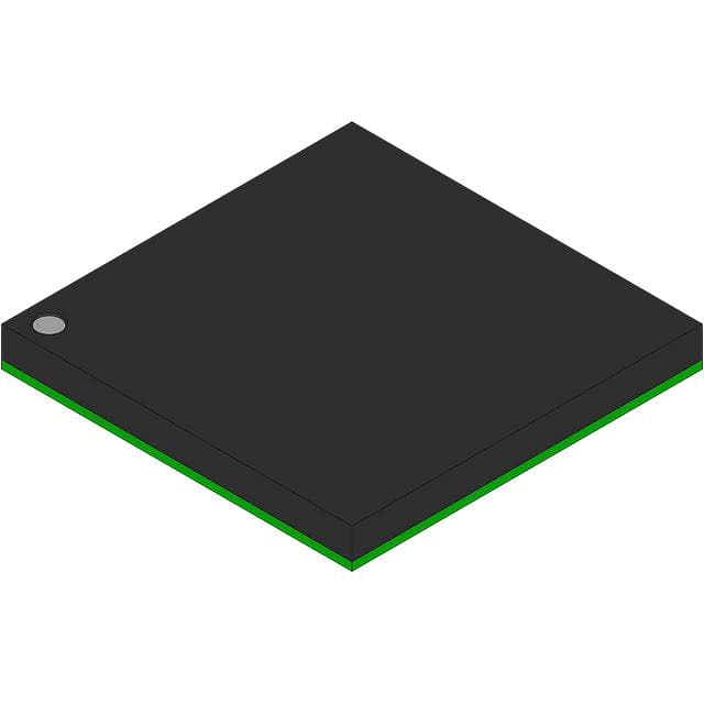
- Part No.:
- DP83815DUJB
- Manufacturer:
- Texas Instruments
- Category:
- Controllers
- Package:
- 160-LBGA
- Datasheet:
-
 DP83815DUJB.pdf
- Description:
- IC MEDIA ACCESS CONTROL 160-LBGA
- Quantity:
- Payment:

- Shipping:

Inventory:2,268
Please send an inquiry. Send us your inquiry, and we will respond immediately.
Product details
Overview
DP83815DUJB from National Semiconductor is a single-chip 10/100 Mb/s PCI Ethernet MAC+PHY (MacPhyter™) in 160-pin LBGA (UJB) package, integrating IEEE 802.3/802.3u-compliant MAC, 3.3V CMOS PHY, 2 KB Tx/Rx FIFOs, and Wake-on-LAN support. It targets low-cost PC motherboards, adapter cards, and embedded systems requiring full-duplex operation, auto-negotiation, and MII interface capability.
For engineers reviewing the DP83815DUJB datasheet, DP83815DUJB pinout, DP83815DUJB application, or DP83815DUJB equivalent, key selection considerations include its integrated 10BASE-T/100BASE-TX transceiver, PCI V2.2 bus mastering up to 128-dword bursts, IEEE 802.3x flow control, VLAN/long-frame support, and power management compliance with ACPI v1.0 and PC98/PC99.
Technical Context
The DP83815DUJB implements a fully integrated PCI MAC/BIU with bus-mastering DMA, supporting burst transfers up to 512 bytes and compliant with PC 97/98/99 hardware design guides. Its physical layer includes ANSI X3.263-compliant TP-PMD with adaptive equalization, baseline wander compensation, and full IEEE 802.3u auto-negotiation.
It features dual-mode operation: native internal PHY for 10/100 twisted-pair connectivity and optional MII interface for external PHY attachment. Power management includes D0–D3cold states, WOL event filtering (Magic Packet™, directed packets, ARP, VLAN), and CLKRUNN-controlled clock gating.
Key Specifications
| Parameter | Value and Actual Design Meaning |
|---|---|
| Data Rate | 10/100 Mb/s full-duplex operation with minimum interframe gap - enables simultaneous transmit/receive at both legacy and Fast Ethernet speeds. |
| PCI Interface | V2.2 33 MHz bus mastering with up to 128-dword (512-byte) bursts - reduces host CPU overhead via descriptor-driven DMA transfers. |
| PHY Integration | Fully integrated 3.3V CMOS 10BASE-T and 100BASE-TX transceivers with auto-negotiation - eliminates need for external PHY in standard twisted-pair applications. |
| Memory Buffers | 2 KB dedicated transmit FIFO + 2 KB dedicated receive FIFO - supports packet bursting and mitigates host latency jitter. |
| Power Modes | D0 (561 mW), WOL (380 mW), Sleep (33 mW) - enables system-level power savings while retaining network responsiveness. |
| Management Interface | MII serial management (MDC/MDIO) with 32 internal PHY registers - allows runtime configuration of link parameters and status monitoring. |
| Wake Events | Supports Magic Packet™, directed packets, VLAN, ARP, pattern match, and PHY status change - provides granular WOL trigger control per OEM requirements. |
Pinout & Package
DP83815DUJB is packaged in a 160-pin LBGA (UJB160A) with 1.0 mm pitch, designed for high-density PCB layouts and thermal reliability in embedded and desktop platforms.
| Pin/Terminal | Circuit Role | Design Meaning |
|---|---|---|
| AD[31:0] | Address/Data Bus | Multiplexed 32-bit address/data lines for PCI transactions; supports Little/Big Endian modes with byte-enable control via CBEN[3:0]. |
| CBEN[3:0] | Command/Byte Enable | Defines bus command during address phase; selects active byte lanes (0–3) during data phase for precise data alignment. |
| PCICLK | PCI Clock Input | 33 MHz max reference clock; rising edge synchronizes all PCI bus phases including address latching and data sampling. |
| INTAN | Interrupt Output | Open-drain active-low interrupt signal tied to PCI INTA#; asserted on configurable events (Rx/Tx completion, errors, WOL). |
| PMEN/CLKRUNN | Power Management Event / Clock Run | Dual-function pin: signals PME events in D3hot/D3cold; or controls dynamic clock gating when CLKRUN_EN bit is set. |
| MDC / MDIO | MII Management Interface | 2.5 MHz serial clock (MDC) and bidirectional data (MDIO) for reading/writing internal PHY registers and external MII devices. |
| RXDV / RXD[3:0] / RXCLK | MII Receive Interface | Nibble-aligned synchronous receive path: RXDV validates frame boundaries; RXCLK = 25 MHz (100 Mbps) or 2.5 MHz (10 Mbps). |
| TXEN / TXD[3:0] / TXCLK | MII Transmit Interface | Transmit enable and 4-bit nibble data driven synchronous to TXCLK; supports MII-compliant external PHY connection. |
Key Features
| Feature | Design Value |
|---|---|
| IEEE 802.3/802.3u Compliance | Fully implements MAC and PHY layers for 10BASE-T and 100BASE-TX, including auto-negotiation, flow control, and error recovery per spec. |
| Flexible Rx Packet Filtering | Single-address perfect filter with MSb masking, 512-entry multicast/unicast hash table, and deep packet pattern matching for up to 4 unique byte patterns. |
| On-chip Statistics Engine | Gathers RFC 1213 (MIB-II), RFC 1398 (Ether-like MIB), and IEEE 802.3 LME counters - offloads SNMP polling and diagnostics from host CPU. |
| EEPROM Auto-Load | Serial EEPROM port loads configuration (MAC address, PHY settings, WOL filters) at power-on - enables field-programmable device identity and behavior. |
| Flash/PROM Boot Support | Dedicated boot ROM interface allows remote firmware initialization and PXE boot capability - essential for diskless workstations and thin clients. |
| Low-Power WOL Operation | Draws only 380 mW in WOL mode while monitoring link activity and packet patterns - extends standby battery life in portable/embedded designs. |
Applications
| Desktop PC Motherboard LAN | Industrial Embedded Controller |
|---|---|
Use Scenario: Integrated 10/100 Ethernet on consumer motherboard with BIOS-based network boot and remote management. IC Role / Device Role / Timing Role: Primary MAC+PHY controller handling PCI-to-Ethernet bridging, auto-negotiation, and WOL packet detection. Use Value: Eliminates discrete MAC+PHY BOM cost and layout complexity while delivering PC99-compliant power management and PXE boot. |
Use Scenario: Networked PLC or HMI unit operating in factory automation with deterministic Ethernet I/O and firmware update over LAN. IC Role / Device Role / Timing Role: Deterministic Ethernet endpoint with MII option for custom PHY tuning and real-time packet timestamping via register-accessible counters. Use Value: Enables IEEE 1588-ready time synchronization through precise MIB-II counter access and low-jitter 25 MHz RXCLK output. |
| PCI Network Adapter Card | Legacy System Upgrade Module |
Use Scenario: Low-profile add-in card for legacy servers requiring Gigabit-predecessor 100BASE-TX connectivity and driver compatibility. IC Role / Device Role / Timing Role: PCI bus master with descriptor-based DMA, supporting Windows/Linux NDIS miniport drivers via standard register map. Use Value: Delivers plug-and-play compatibility with existing OS drivers while reducing host interrupt load via burst transfers and interrupt coalescing. |
Use Scenario: Retrofit module for aging kiosk or medical terminal needing secure remote diagnostics without board redesign. IC Role / Device Role / Timing Role: Secure network interface with WOL-enabled remote wake, encrypted Magic Packet™ filtering, and EEPROM-stored MAC lockdown. Use Value: Extends product lifecycle by adding modern network manageability to legacy hardware using minimal PCB space and no FPGA logic. |
Equivalent & Alternatives
The following parts are listed as comparable options for similar Ethernet MAC+PHY applications.
| Alternative Part | Technical Difference | Application Difference | Selection Advice |
|---|---|---|---|
| RTL8139C(L) | PCI 32-bit 33 MHz MAC+PHY; no MII interface; simpler WOL filtering (Magic Packet™ only); 128-pin LQFP package. | Lacks VLAN support, long-frame handling, and deep packet pattern matching; lower integration density than DP83815DUJB. | Choose for cost-sensitive, non-VLAN, non-WOL-intensive applications where driver ubiquity outweighs feature depth. |
| DM9000AEP | Non-PCI parallel/ISA bus interface; 16-bit host interface; external PHY required; 80-pin LQFP; no auto-negotiation engine. | Requires external PHY and glue logic; suited for microcontroller-based systems rather than x86 PCI hosts. | Choose only for non-PCI architectures (e.g., ARM9 with local bus) where PCI compatibility is not required. |
Compared with RTL8139C(L) and DM9000AEP, DP83815DUJB offers superior integration (native PHY + MII), richer WOL filtering, VLAN/long-frame support, and tighter power management compliance - making it optimal for PC-class and industrial PCI-based designs demanding feature completeness and standards adherence.
Availability
DP83815DUJB is available at Aetrix Electronics and suitable for desktop motherboard integration, industrial embedded controllers, and PCI network adapter cards requiring stable component supply, long-term lifecycle support, and traceable sourcing.
Supply support for DP83815DUJB includes scheduled delivery planning, volume procurement assistance, BOM continuity management, traceable sourcing, and lifecycle availability coordination for OEM customers, industrial embedded developers, connected-device designers, and electronics production programs.
Manufacturer
National Semiconductor was a U.S.-based semiconductor company specializing in analog, interface, and mixed-signal ICs before its acquisition by Texas Instruments in 2011. It pioneered highly integrated communication solutions for PC and embedded markets.
The DP83815DUJB belongs to National's MacPhyter™ family of integrated Ethernet controllers, designed specifically to reduce BOM cost and PCB area in volume PC and embedded applications while maintaining full IEEE compliance and robust power management.
FAQ
What is the package type and pin count of DP83815DUJB?
DP83815DUJB uses a 160-pin LBGA package (NS package code UJB160A) with 1.0 mm ball pitch. This package is distinct from the 144-pin LQFP variant (DP83815DVNG) and is optimized for thermal performance and high-density routing in desktop and embedded motherboard designs. The LBGA footprint supports automated assembly and improved signal integrity for PCI bus timing.
Does DP83815DUJB support both 10BASE-T and 100BASE-TX physical layers?
Yes, DP83815DUJB integrates a fully compliant IEEE 802.3u 100BASE-TX transceiver and IEEE 802.3 10BASE-T transceiver in a single die. It supports auto-negotiation between both speeds, full-duplex operation at either rate, and includes adaptive equalization and baseline wander compensation for reliable 100 Mbps operation over Category 5 cabling up to 100 meters.
Can DP83815DUJB operate with an external PHY via MII?
Yes, DP83815DUJB supports Media Independent Interface (MII) operation when CFG:EXT_PHY is enabled. Pins MDC, MDIO, RXD[3:0], RXDV, RXER, CRS, COL, TXD[3:0], TXEN, and TXCLK become active for connection to external PHYs. This mode disables the internal PHY and allows customization for fiber, AUI, or specialized copper interfaces.
What power management features does DP83815DUJB provide?
DP83815DUJB complies with ACPI v1.0 and PCI Power Management Specification v1.1, supporting D0–D3cold states. It delivers 561 mW in D0, 380 mW in WOL mode, and 33 mW in sleep mode. Wake-on-LAN triggers include Magic Packet™, directed packets, VLAN, ARP, and PHY status change - all configurable via EEPROM or register writes.
How is configuration data loaded into DP83815DUJB at startup?
DP83815DUJB features a serial EEPROM port that auto-loads configuration data at power-on reset. This includes MAC address, PHY settings, WOL filter patterns, and interrupt polarity. The EEPROM interface uses MA3/EEDI, MA4/EECLK, and MD4/EEDO pins (LBGA pins C1, A1, C2), enabling field-programmable identity and behavior without firmware intervention.
DP83815DUJB Specifications
- Product attributes
- Attribute value
- Manufacturer:
- Texas Instruments
- Package/Case:
- 160-LBGA
- Programmable:
- Not Verified
- Protocol:
- Ethernet
- Function:
- Controller
- Interface:
- PCI
- Standards:
- 10/100 Base-T/TX PHY
- Voltage - Supply:
- 3.3V
- Current - Supply:
- 170mA
- Operating Temperature:
- 0°C ~ 70°C
- Supplier Device Package:
- 160-LBGA (15x15)
- Grade:
- -
- Qualification:
- -
DP83815DUJB FAQ
1.How can I place an order for DP83815DUJB through Aetrix?
Please submit a Request for Quotation (RFQ) for DP83815DUJB on Aetrix. Our sales agent will provide a competitive quotation and guide you through the order confirmation once you accept the terms.
2.Are the price and stock information for DP83815DUJB reliable?
The price and inventory of DP83815DUJB are updated periodically and may fluctuate due to market conditions. Stock and pricing data are typically refreshed every 24 hours. Quotation validity for DP83815DUJB is usually 5 days.
3.What payment methods are accepted for DP83815DUJB?
We accept Wire Transfer, PayPal, Credit Card, Western Union, MoneyGram, and Escrow for DP83815DUJB transactions.
Note: Certain payment methods may incur a processing fee.
4.How is shipping managed for DP83815DUJB?
DP83815DUJB orders can be shipped via leading logistics carriers, including DHL, UPS, FedEx, TNT, or Registered Mail.
Once your DP83815DUJB order is processed, you will receive an email with the shipment details and tracking number.
Note: Tracking information may take up to 24 hours to appear. Express delivery typically takes 3–5 business days.
5.How can I obtain technical support or documentation for DP83815DUJB?
For technical support, including DP83815DUJB datasheets, pinout diagrams, or application guidance, please contact our engineering support team. They can provide detailed documentation and assistance for your DP83815DUJB requirements.
6.How does Aetrix verify that DP83815DUJB is sourced from the original manufacturer or authorized distributors?
All DP83815DUJB products on Aetrix are procured from qualified distributors and authorized channels. Our dedicated quality assurance team conducts strict verification, including traceability checks and, if necessary, third-party testing. This ensures that DP83815DUJB meets industry standards.
7.What is the process for return or replacement of DP83815DUJB?
All DP83815DUJB units undergo pre-shipment inspection (PSI). If there is an issue with DP83815DUJB, returns or replacements are accepted under the following conditions:
1.Quantity discrepancies, incorrect items, or visible external defects (such as breakage or corrosion), acknowledged by Aetrix.
2.The issue is reported within 90 days of delivery.
3.The DP83815DUJB part is unused and in its original packaging.
Return procedure for DP83815DUJB:
1.Submit a request within 90 days.
2.Obtain a Return Material Authorization (RMA) from Aetrix.
DP83815DUJB Tags

-
PTN5150AHXMP
NXP Semiconductors

-
USB3740B-AI9-TR
Microchip Technology

-
USB3740B-AI2-TR
Microchip Technology

-
USB3300-EZK-TR
Microchip Technology
-
USB3300-EZK
Microchip Technology

-
FUSB340TMX
onsemi

-
FUSB302BMPX
onsemi

-
DP83826IRHBR
Texas Instruments

-
MCP2518FDT-E/QBB
Microchip Technology
-
FUSB302MPX
onsemi

-
MCP2518FDT-E/SL
Microchip Technology

-
FT260Q-R
FTDI, Future Technology Devices International Ltd
Tech Hub

A practical engineering guide to 3.3V and 5V logic compatibility, input thresholds, resistor dividers, translator ICs, MOSFET level shifting, I2C pull-ups, timing limits and power-sequencing risks.

The 74HC595 uses push-pull logic outputs, while the TPIC6B595 uses 50 V open-drain DMOS sinks for higher-power loads. This guide compares timing, current limits, 3.3 V interfacing, load wiring, thermal…

The 74HC595 converts serial data into eight stable parallel outputs. This guide covers pin functions, shift and storage timing, OE and MR behavior, drive-current limits, cascading, voltage compatibilit…

A technical comparison of level-sensitive latches and edge-triggered flip-flops, covering timing windows, setup and hold limits, master–slave operation, time borrowing, race-through, HDL inference and…

A D latch stores one bit while Enable controls when data can pass. This reference covers gate-level operation, truth tables, transparency, setup and hold timing, LE versus OE, common ICs and practical …

An SR latch stores one bit through cross-coupled feedback. This engineering reference covers NOR and NAND implementations, truth tables, forbidden-state recovery, gated operation, switch debouncing, fa…

Latch circuits retain one bit through feedback. This technical reference covers SR and D latches, truth tables, transparency, timing limits, latch-versus-flip-flop behavior, applications and common log…

An engineering guide to LED driver operation, constant-current and constant-voltage outputs, linear and switching topologies, dimming, IC selection, calculations, replacement compatibility, and fault c…

Operational amplifier guide covering op amp basics, feedback, ideal vs real op amps, common configurations, buffer circuits, offset, bias current, gain-bandwidth, slew rate, rail-to-rail limits and sel…

Jumper cables guide covering safe connection order, red and black clamp placement, final ground connection, cable gauge, length, clamp quality, copper vs CCA cables, jump starter comparison and battery…


