
 My Inquiry
 My Account


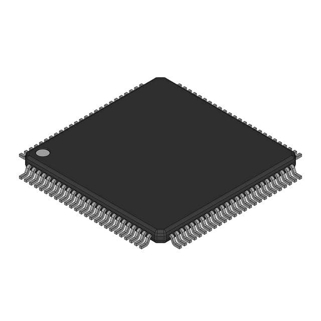
Texas Instruments DP83840AVCE
- Part No.:
- DP83840AVCE
- Manufacturer:
- Texas Instruments
- Category:
- Controllers
- Package:
- 100-BQFP
- Datasheet:
-
 DP83840AVCE.pdf
- Description:
- IC ETHERNET PHYS LAYER 100QFP
- Quantity:
- Payment:

- Shipping:

Inventory:3,794
Please send an inquiry. Send us your inquiry, and we will respond immediately.
Product details
Overview
DP83840AVCE from National Semiconductor is a 10/100 Mb/s Ethernet Physical Layer (PHY) transceiver IC supporting IEEE 802.3 10BASE-T and IEEE 802.3u 100BASE-X standards. It integrates dual-speed ENDEC, clock recovery, PCS, auto-negotiation, and MII interface, operating with category 5 UTP, type 1 STP, or fiber optic media. It serves as the physical layer bridge between MAC and PMD in embedded LAN controllers and industrial Ethernet nodes.
For engineers reviewing the DP83840AVCE datasheet, DP83840AVCE pinout, DP83840AVCE application, or DP83840AVCE equivalent, key selection considerations include its 100-pin PQFP package, IEEE 802.3u-compliant MII and serial management interface, full-duplex support at both speeds, integrated 100 Mb/s clock recovery, and IEEE 1149.1 boundary-scan capability.
Technical Context
The DP83840AVCE implements a dual-speed architecture with separate 10BASE-T transceiver and 100BASE-X PCS modules sharing a unified MII interface and auto-negotiation engine. Its clock recovery module operates without external filters, and its scrambler/descrambler supports multi-PHY applications via individualized seed configuration.
It supports configurable node/repeater modes, programmable loopback (local 100BASE-TX, encoder/alignment/scrambler bypass), and flexible LED control with monostable timing for visibility. The device uses National's BiCMOS process and integrates FDDI-derived clock generation and stream cipher logic.
Key Specifications
| Parameter | Value and Actual Design Meaning |
|---|---|
| Data Rates | 10 Mb/s (10BASE-T) and 100 Mb/s (100BASE-TX/FX) - enables backward-compatible, scalable Ethernet connectivity |
| Interface Standard | IEEE 802.3u-compliant Media Independent Interface (MII) - ensures interoperability with diverse MAC controllers |
| Auto-Negotiation | IEEE 802.3u-compliant - automatically selects speed and duplex mode with link partners |
| Power Supply | 3.3 V core and I/O - compatible with modern low-voltage system designs |
| Package | 100-pin JEDEC metric PQFP - surface-mountable with standard PCB layout rules |
| Clock Recovery | Integrated 100 Mb/s clock recovery requiring no external filter components - reduces BOM count and board area |
| Test Support | IEEE 1149.1 JTAG boundary-scan - enables production testability and debug without intrusive probing |
Pinout & Package
DP83840AVCE is housed in a 100-pin JEDEC metric PQFP package (14 mm × 20 mm, 0.65 mm pitch), optimized for high-density Ethernet PHY placement with thermal and signal integrity considerations.
| Pin/Terminal | Circuit Role | Design Meaning |
|---|---|---|
| TXD[3:0] | MII Transmit Data Input | Nibble-wide parallel data path for 10/100 Mb/s transmit; TXD[0] repurposed as serial input in 10 Mb/s serial mode |
| RXD[3:0] | MII Receive Data Output | Nibble-wide parallel receive data synchronized to RX_CLK; RXD[0] used as serial output in 10 Mb/s serial mode |
| MDIO / MDC | Serial Management Interface | Bi-directional register access interface (max 2.5 MHz) for PHY configuration and status monitoring |
| TD+/TD−, RD+/RD−, SD+/SD− | 100 Mb/s Serial PMD Interface | Differential ECL-level signals for connection to DP83223 or compatible transceivers |
| TXU+/TXU−, TXS+/TXS−, RXI+/RXI− | 10 Mb/s UTP/STP Interface | Direct-drive differential outputs and inputs for 10BASE-T physical layer signaling |
| LED1–LED5 | CMOS LED Drivers | Active-low outputs with monostable pulse extension (~50 ms) for reliable visual link/activity indication |
| TMS/TCK/TDI/TDO/TRST | JTAG Test Access Port | Full IEEE 1149.1 boundary-scan support for system-level diagnostics and manufacturing test |
Key Features
| Feature | Design Value |
|---|---|
| Integrated 100 Mb/s clock recovery | Eliminates need for external analog filters, simplifying layout and improving reliability across temperature/voltage |
| Programmable node/repeater mode | Enables single hardware design to serve as either endpoint or hub component via REPEATER pin configuration |
| Three independent bypass modes (BP4B5B, BPALIGN, BPSCR) | Supports 100BASE-FX operation and diagnostic testing by selectively disabling encoder, alignment, or scrambler functions |
| Flexible PHY address strapping (PHYAD[4:0]) | Allows up to 31 unique addresses on shared MII bus, enabling multi-PHY systems without address conflict |
| Monostable LED drivers | Guarantees minimum 50 ms LED ON time even for 64-byte packets, ensuring human-visible link/activity feedback |
Applications
| Industrial Control Network Node | Legacy Equipment Ethernet Retrofit |
|---|---|
Use Scenario: Integrating PLCs, HMIs, and remote I/O into deterministic factory-floor Ethernet networks using existing 10BASE-T infrastructure. IC Role / Device Role / Timing Role: PHY layer translator between legacy MAC controllers and twisted-pair physical media, handling Manchester encoding/decoding and carrier sensing. Use Value: Enables drop-in upgrade of aging automation hardware with IEEE 802.3 compliance, auto-negotiation fallback, and robust 10 Mb/s link integrity detection. |
Use Scenario: Adding Ethernet connectivity to legacy instrumentation or medical devices originally designed for RS-232 or proprietary serial interfaces. IC Role / Device Role / Timing Role: Standalone physical layer interface bridging microcontroller UART/MAC peripherals to RJ-45 ports via MII or simplified serial mode. Use Value: Provides certified 10/100 Mb/s PHY functionality with minimal external components-no magnetics required for basic evaluation, and full IEEE 1149.1 test access for field service. |
| Multi-Port Industrial Switch ASIC Companion | 100BASE-TX Repeater Hub Module |
Use Scenario: Serving as one of multiple PHYs in a custom 8-port managed switch ASIC reference design targeting harsh environments. IC Role / Device Role / Timing Role: Dedicated 100 Mb/s PHY per port with independent auto-negotiation, LED status, and boundary-scan test access. Use Value: Individualized scrambler seed and strappable PHY addresses prevent inter-port interference; JTAG chain enables full-board test coverage without probe fixtures. |
Use Scenario: Building compact, fanless 4-port repeater hubs for lab or educational use where full switching intelligence is unnecessary. IC Role / Device Role / Timing Role: Repeater-mode PHY performing signal regeneration, collision detection, and carrier sense forwarding across ports. Use Value: REPEATER pin configures CRS behavior per IEEE 802.3u/D5.3 CIM requirements; COL and LED5 provide real-time collision visibility for teaching and troubleshooting. |
Equivalent & Alternatives
The following parts are listed as comparable options for similar Ethernet PHY applications.
| Alternative Part | Technical Difference | Application Difference | Selection Advice |
|---|---|---|---|
| DP83840A | Original version; identical electrical and functional spec to DP83840AVCE except for minor packaging marking | No difference - same pinout, registers, timing, and feature set | Select DP83840AVCE for guaranteed availability and documented VCE-grade qualification |
| LAN83C185 | Lantronix implementation with identical MII interface and 10/100 PHY function but different register map and LED control logic | Requires firmware adaptation for register access and status interpretation; no JTAG support | Choose only when migrating legacy Lantronix-based designs; not drop-in compatible |
Compared with DP83840A and LAN83C185, the DP83840AVCE offers identical core functionality with verified VCE-grade reliability, full JTAG testability, and seamless register compatibility-making it the preferred choice for new designs requiring long-term supply stability and production test coverage.
Availability
DP83840AVCE is available at Aetrix Electronics and suitable for industrial control network nodes, legacy equipment Ethernet retrofit, multi-port switch modules, and 100BASE-TX repeater hubs requiring stable component supply and long-lifecycle support.
Supply support for DP83840AVCE includes scheduled delivery planning, volume procurement assistance, BOM continuity management, traceable sourcing, and lifecycle availability coordination for OEM customers, industrial embedded developers, connected-device designers, and electronics production programs.
Manufacturer
National Semiconductor was a pioneering analog and mixed-signal semiconductor company, acquired by Texas Instruments in 2011. It developed foundational Ethernet PHY, data converter, and power management technologies widely adopted in industrial and communications systems.
The DP83840AVCE belongs to National's early-generation 10/100 Mb/s Ethernet PHY product line, engineered specifically for cost-sensitive, high-reliability embedded LAN applications requiring IEEE 802.3u compliance and minimal external component count.
FAQ
What is the primary function of the DP83840AVCE in an Ethernet system?
The DP83840AVCE serves as a dual-speed Physical Layer (PHY) transceiver, converting digital MAC-layer data from the MII interface into analog 10BASE-T or 100BASE-X signals for transmission over copper or fiber media. It handles encoding/decoding, clock recovery, auto-negotiation, and signal conditioning-enabling interoperable, standards-compliant Ethernet connectivity. Its role is strictly physical layer translation, not packet processing or switching logic.
Does the DP83840AVCE support both half-duplex and full-duplex operation at 10 Mb/s and 100 Mb/s?
Yes, the DP83840AVCE supports full-duplex and half-duplex operation at both 10 Mb/s and 100 Mb/s, as defined by IEEE 802.3u. Full-duplex mode disables collision detection (COL remains low), while half-duplex enables it. Duplex mode is determined during auto-negotiation or via forced configuration using AN0/AN1 pins. The DP83840AVCE implements all required timing, carrier sense, and collision logic per standard.
Can the DP83840AVCE operate without an external crystal or oscillator?
No-the DP83840AVCE requires either a 50 MHz TTL oscillator on OSCIN (pin 2) or a 20 MHz crystal across X1/X2 (pins 33/34) to generate internal clocks. The 50 MHz input feeds the PLL for 100 Mb/s operation; the 20 MHz crystal supports 10 Mb/s timing and auto-negotiation. REF IN (pin 86) may accept a 25 MHz external clock as alternative, but no clock source can be omitted without functional failure.
How does the DP83840AVCE handle PHY addressing in multi-device MII configurations?
The DP83840AVCE uses five dedicated PHY address pins (PHYAD[4:0], mapped to pins RX_ER, SPEED_100, CRS, ENCSEL, LBEN) to configure a unique 5-bit address. Pull-up/down resistors set each bit at power-up, latching the value into the PHY Address Register (address 19h). This allows up to 31 distinct PHYs on a shared MII bus-critical for multi-port switches or modular systems-without software address conflicts or MDIO arbitration overhead.
Is the DP83840AVCE pin-compatible with newer National Semiconductor or TI Ethernet PHYs?
No-the DP83840AVCE is not pin-compatible with later-generation PHYs such as the DP83865 or TLK100 series. Its 100-pin PQFP footprint, ECL-level PMD signals (TD+/RD+/SD+), and dedicated 10 Mb/s analog interfaces differ fundamentally from modern 48-pin QFN devices with integrated magnetics drivers and digital SGMII/RMII interfaces. Migration requires PCB redesign and firmware register mapping updates.
DP83840AVCE Specifications
- Product attributes
- Attribute value
- Manufacturer:
- Texas Instruments
- Package/Case:
- 100-BQFP
- Programmable:
- Not Verified
- Protocol:
- Ethernet
- Function:
- Physical Layer Controller
- Interface:
- -
- Standards:
- 10/100 Base-T/TX PHY
- Voltage - Supply:
- 4.75V ~ 5.25V
- Current - Supply:
- 335mA
- Operating Temperature:
- 0°C ~ 70°C
- Supplier Device Package:
- 100-PQFP (14x20)
- Grade:
- -
- Qualification:
- -
DP83840AVCE FAQ
1.How can I place an order for DP83840AVCE through Aetrix?
Please submit a Request for Quotation (RFQ) for DP83840AVCE on Aetrix. Our sales agent will provide a competitive quotation and guide you through the order confirmation once you accept the terms.
2.Are the price and stock information for DP83840AVCE reliable?
The price and inventory of DP83840AVCE are updated periodically and may fluctuate due to market conditions. Stock and pricing data are typically refreshed every 24 hours. Quotation validity for DP83840AVCE is usually 5 days.
3.What payment methods are accepted for DP83840AVCE?
We accept Wire Transfer, PayPal, Credit Card, Western Union, MoneyGram, and Escrow for DP83840AVCE transactions.
Note: Certain payment methods may incur a processing fee.
4.How is shipping managed for DP83840AVCE?
DP83840AVCE orders can be shipped via leading logistics carriers, including DHL, UPS, FedEx, TNT, or Registered Mail.
Once your DP83840AVCE order is processed, you will receive an email with the shipment details and tracking number.
Note: Tracking information may take up to 24 hours to appear. Express delivery typically takes 3–5 business days.
5.How can I obtain technical support or documentation for DP83840AVCE?
For technical support, including DP83840AVCE datasheets, pinout diagrams, or application guidance, please contact our engineering support team. They can provide detailed documentation and assistance for your DP83840AVCE requirements.
6.How does Aetrix verify that DP83840AVCE is sourced from the original manufacturer or authorized distributors?
All DP83840AVCE products on Aetrix are procured from qualified distributors and authorized channels. Our dedicated quality assurance team conducts strict verification, including traceability checks and, if necessary, third-party testing. This ensures that DP83840AVCE meets industry standards.
7.What is the process for return or replacement of DP83840AVCE?
All DP83840AVCE units undergo pre-shipment inspection (PSI). If there is an issue with DP83840AVCE, returns or replacements are accepted under the following conditions:
1.Quantity discrepancies, incorrect items, or visible external defects (such as breakage or corrosion), acknowledged by Aetrix.
2.The issue is reported within 90 days of delivery.
3.The DP83840AVCE part is unused and in its original packaging.
Return procedure for DP83840AVCE:
1.Submit a request within 90 days.
2.Obtain a Return Material Authorization (RMA) from Aetrix.
DP83840AVCE Tags

-
PTN5150AHXMP
NXP Semiconductors

-
USB3740B-AI9-TR
Microchip Technology

-
USB3740B-AI2-TR
Microchip Technology

-
USB3300-EZK-TR
Microchip Technology
-
USB3300-EZK
Microchip Technology

-
FUSB340TMX
onsemi

-
FUSB302BMPX
onsemi

-
DP83826IRHBR
Texas Instruments

-
MCP2518FDT-E/QBB
Microchip Technology
-
FUSB302MPX
onsemi

-
MCP2518FDT-E/SL
Microchip Technology

-
FT260Q-R
FTDI, Future Technology Devices International Ltd
Tech Hub

A practical engineering guide to 3.3V and 5V logic compatibility, input thresholds, resistor dividers, translator ICs, MOSFET level shifting, I2C pull-ups, timing limits and power-sequencing risks.

The 74HC595 uses push-pull logic outputs, while the TPIC6B595 uses 50 V open-drain DMOS sinks for higher-power loads. This guide compares timing, current limits, 3.3 V interfacing, load wiring, thermal…

The 74HC595 converts serial data into eight stable parallel outputs. This guide covers pin functions, shift and storage timing, OE and MR behavior, drive-current limits, cascading, voltage compatibilit…

A technical comparison of level-sensitive latches and edge-triggered flip-flops, covering timing windows, setup and hold limits, master–slave operation, time borrowing, race-through, HDL inference and…

A D latch stores one bit while Enable controls when data can pass. This reference covers gate-level operation, truth tables, transparency, setup and hold timing, LE versus OE, common ICs and practical …

An SR latch stores one bit through cross-coupled feedback. This engineering reference covers NOR and NAND implementations, truth tables, forbidden-state recovery, gated operation, switch debouncing, fa…

Latch circuits retain one bit through feedback. This technical reference covers SR and D latches, truth tables, transparency, timing limits, latch-versus-flip-flop behavior, applications and common log…

An engineering guide to LED driver operation, constant-current and constant-voltage outputs, linear and switching topologies, dimming, IC selection, calculations, replacement compatibility, and fault c…

Operational amplifier guide covering op amp basics, feedback, ideal vs real op amps, common configurations, buffer circuits, offset, bias current, gain-bandwidth, slew rate, rail-to-rail limits and sel…

Jumper cables guide covering safe connection order, red and black clamp placement, final ground connection, cable gauge, length, clamp quality, copper vs CCA cables, jump starter comparison and battery…


