
 My Inquiry
 My Account


Texas Instruments DP83848JSQ/NOPB
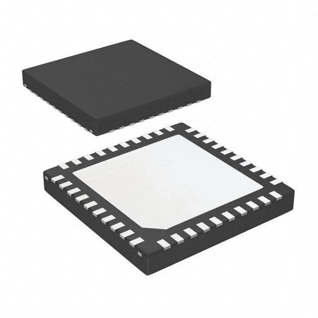
- Part No.:
- DP83848JSQ/NOPB
- Manufacturer:
- Texas Instruments
- Category:
- Drivers, Receivers, Transceivers
- Package:
- 40-WFQFN Exposed Pad
- Datasheet:
-
 DP83848JSQ/NOPB.pdf
- Description:
- IC TRANSCEIVER 1/1 40WQFN
- Quantity:
- Payment:

- Shipping:

Inventory:1,825
Please send an inquiry. Send us your inquiry, and we will respond immediately.
Product details
Overview
DP83848JSQ/NOPB from Texas Instruments is a single-port 10/100 Mbps Ethernet PHY transceiver in a 40-pin WQFN package, supporting both MII and RMII MAC interfaces, Auto-MDIX, IEEE 802.3-compliant 10BASE-T/100BASE-TX physical layer operation, and 3.3-V I/O interface. It delivers error-free operation beyond 137 meters over Cat-5 cable and integrates adaptive equalization and baseline wander compensation for robust signal integrity in industrial automation and embedded networking applications.
For engineers reviewing the DP83848JSQ/NOPB datasheet, DP83848JSQ/NOPB pinout, DP83848JSQ/NOPB application, or DP83848JSQ/NOPB equivalent, key selection considerations include its dual-interface flexibility (MII/RMII), commercial-grade temperature range (0°C to 70°C), integrated LED control for link/speed indication, 4-kV HBM ESD rating, and compatibility with standard 25-MHz crystal or 50-MHz oscillator reference clocks.
Technical Context
The DP83848JSQ/NOPB implements a full IEEE 802.3-compliant PHY layer with ENDEC, PCS, and TP-PMD sublayers - including ANSI X3.263–compliant 100BASE-TX transceivers, 10BASE-T transceivers, and adaptive analog front-end circuitry. Its Auto-MDIX function operates transparently at both 10 and 100 Mbps without software intervention.
It supports hardware-strapped configuration of PHY address (5-bit), MII/RMII mode (via RX_DV pin), LED behavior (Mode 1/2), and MDIX enable/disable - all latched at hardware reset. The device uses internal pulldown/pullup resistors on strap pins, requiring only optional 2.2-kΩ external resistors to override defaults.
Key Specifications
| Parameter | Value and Actual Design Meaning |
|---|---|
| Data Rate | 10/100 Mbps full/half-duplex - supports legacy 10BASE-T and high-speed 100BASE-TX links with automatic speed negotiation. |
| Interface | MII or RMII (configurable via RX_DV strap) - enables flexible MAC integration with minimal pin count or timing overhead. |
| Supply Voltage | 3.3 V ±0.3 V - single-supply operation simplifies power design; separate IOVDD33, AVDD33, and DGND/AGND domains ensure noise isolation. |
| ESD Rating | ±4 kV HBM - exceeds IEC 61000-4-2 Level 3 requirements, enabling reliable deployment in factory-floor environments. |
| Cable Reach | >137 m on Cat-5 - achieved via adaptive equalization and baseline wander compensation, eliminating need for external line drivers in most industrial settings. |
| Operating Temp | 0°C to 70°C - commercial-grade thermal specification suitable for peripheral devices, mobile gateways, and non-extreme industrial enclosures. |
| Package | 40-pin WQFN (6 mm × 6 mm) - compact footprint ideal for space-constrained PCBs in embedded routers and IoT edge nodes. |
Pinout & Package
The DP83848JSQ/NOPB is housed in a 40-pin WQFN package (RTA) with 0.5-mm pitch and wettable flanks. Thermal pad (DAP) on underside requires solder connection to PCB ground plane for optimal thermal performance and EMI control.
| Pin/Terminal | Circuit Role | Design Meaning |
|---|---|---|
| TXD[3:0] (Pins 4–7) | MII Transmit Data Inputs | Accept nibble-wide parallel data synchronous to TX_CLK; support 10/100 Mbps MII timing with setup/hold constraints defined per IEEE 802.3. |
| RXD[3:0] (Pins 36–39) | MII Receive Data Outputs | Drive valid nibble data when RX_DV is asserted; output timing referenced to RX_CLK (2.5 MHz / 25 MHz) and synchronized to recovered clock domain. |
| TD+/TD− (Pins 15/14) | 10/100 Mbps PMD Transmit Pair | Differential 100BASE-TX (1 Vpp) or 10BASE-T (2.5 Vpp) output; Auto-MDIX allows dynamic crossover detection and correction without manual cabling. |
| RD+/RD− (Pins 12/11) | 10/100 Mbps PMD Receive Pair | Differential input pair with programmable signal detect thresholds (1000 mVpk-pk turn-on); supports both 10BASE-T and 100BASE-TX signaling automatically. |
| LED_LINK / LED_SPEED (Pins 22/21) | Configurable Link & Speed Indicators | Open-drain outputs with internal pullup; support Mode 1 (link-only) or Mode 2 (link + activity blink); SPEED LED indicates 100 Mbps (ON) vs. 10 Mbps (OFF). |
| RESET_N (Pin 23) | Active-Low Hardware Reset | Asynchronous reset pulse ≥1 µs forces full register initialization and re-latching of strap options; critical for deterministic boot behavior in embedded systems. |
| X1/X2 (Pins 28/27) | Crystal Oscillator Interface | X1 accepts 25-MHz crystal or 50-MHz CMOS clock; X2 is crystal output - unused when external oscillator is applied; supports precise clock recovery for jitter-sensitive applications. |
Key Features
| Feature | Design Value |
|---|---|
| Auto-MDIX | Eliminates requirement for straight-through vs. crossover cables - reduces field installation errors and simplifies network topology changes. |
| Energy Detection Mode | Enables low-power wake-on-link functionality by detecting presence of valid Ethernet signal without full PHY initialization. |
| Single Register Access for Status | PHY status (link, speed, duplex, auto-neg completion) readable via single MII register read (Register 1), accelerating firmware polling efficiency. |
| 10/100 Mbps Packet BIST | On-chip self-test verifies transmit/receive datapath integrity during production test or field diagnostics without external test equipment. |
| RMII Rev. 1.2 Support | Reduces MAC-to-PHY interface from 16 to 7 pins and eliminates need for TX_CLK/RX_CLK - lowers routing complexity and improves timing margin in high-density designs. |
Applications
| Industrial Ethernet I/O Module | Embedded Wireless Gateway |
|---|---|
Use Scenario: DIN-rail mounted PLC extension module connecting sensors/actuators via 100BASE-TX to central controller over unshielded twisted-pair cabling in factory floor environment. IC Role / Device Role / Timing Role: PHY layer translator between microcontroller's RMII interface and RJ-45 magnetics; provides clock recovery, line encoding/decoding, and ESD-hardened PMD signaling. Use Value: Enables deterministic 100 Mbps communication over >137 m without repeaters; Auto-MDIX prevents miswiring during field maintenance; 4-kV HBM withstands electrostatic discharge common in metal-enclosed industrial cabinets. | Use Scenario: Compact Wi-Fi 6 access point with wired uplink, where space-constrained PCB must integrate Ethernet PHY alongside RF front-end and SoC without thermal derating. IC Role / Device Role / Timing Role: Physical layer interface bridging SoC's MII port to external switch or ISP router; handles 10/100 Mbps auto-negotiation, packet serialization, and differential signaling to magnetics. Use Value: 6 mm × 6 mm WQFN package saves >30% board area versus QFP alternatives; low 264 mW typical power dissipation avoids thermal throttling near RF components; integrated LED drivers reduce BOM count by two discrete drivers. |
| Building Automation Controller | Test & Measurement Equipment |
Use Scenario: HVAC control panel with Ethernet backhaul for remote monitoring, deployed in office ceilings where ambient temperature remains 0–55°C and cable runs exceed 100 m. IC Role / Device Role / Timing Role: Ethernet transceiver interfacing ARM Cortex-M7 MCU to building management system via Cat-5e; performs adaptive equalization to compensate for signal attenuation over long cable runs. Use Value: Error-free operation beyond 137 m eliminates need for mid-span repeaters or fiber conversion; commercial temp grade matches HVAC enclosure specifications; configurable LED outputs provide local link/speed verification without debug tools. | Use Scenario: Portable oscilloscope with LAN-based waveform export and remote control, requiring reliable Ethernet connectivity in lab and field environments subject to ESD events. IC Role / Device Role / Timing Role: PHY component in instrument's communication subsystem, converting parallel MAC data to differential 100BASE-TX signals compliant with IEEE 802.3u. Use Value: ±4 kV HBM ESD protection ensures immunity to operator-handling discharges; single-register status access accelerates firmware response to link loss; MII/RMII flexibility supports future SoC upgrades without PCB redesign. |
Equivalent & Alternatives
The following parts are listed as comparable options for similar Ethernet PHY transceiver applications.
| Alternative Part | Technical Difference | Application Difference | Selection Advice |
|---|---|---|---|
| LAN8720AI-CP | 3.3-V single-port 10/100 PHY in 24-pin QFN; lacks RMII support and integrated LED drivers; lower ESD rating (2 kV HBM). | Better suited for cost-sensitive consumer electronics where RMII isn't required and board space is less constrained. | Select LAN8720AI-CP only if RMII interface and LED drive capability are unnecessary and BOM cost reduction outweighs robustness trade-offs. |
| KSZ8041NL | 3.3-V 10/100 PHY in 48-pin QFN; includes integrated 1.25-V LDO, MII-only interface, and 8-kV ESD rating; no Auto-MDIX in some revisions. | Preferred for automotive-adjacent industrial designs requiring higher ESD immunity and regulated analog supply, but requires additional layout area and lacks DP83848JSQ/NOPB's RMII option. | Choose KSZ8041NL when system-level ESD compliance exceeds 4 kV or when integrated LDO simplifies power architecture - not for RMII-based compact designs. |
Compared with LAN8720AI-CP and KSZ8041NL, the DP83848JSQ/NOPB uniquely balances RMII/MII dual-interface support, integrated LED control, Auto-MDIX, and 4-kV HBM rating in a 6 mm × 6 mm footprint - making it optimal for space- and reliability-critical embedded Ethernet endpoints where interface flexibility and field-deployment robustness are mandatory.
Availability
DP83848JSQ/NOPB is available at Aetrix Electronics and suitable for industrial Ethernet I/O modules, embedded wireless gateways, building automation controllers, and test & measurement equipment requiring stable component supply across multi-year production cycles.
Supply support for DP83848JSQ/NOPB includes scheduled delivery planning, volume procurement assistance, BOM continuity management, traceable sourcing, and lifecycle availability coordination for OEM customers, industrial embedded developers, connected-device designers, and electronics production programs.
Manufacturer
Texas Instruments is a global semiconductor leader specializing in analog, embedded processing, and connectivity solutions, with decades of leadership in Ethernet PHY innovation and industrial-grade reliability.
The DP83848x product line was designed specifically for space-constrained, high-reliability embedded networking applications - emphasizing low power, superior cable reach, and seamless MAC interface flexibility across MII and RMII standards.
FAQ
What is the operating temperature range for DP83848JSQ/NOPB?
The DP83848JSQ/NOPB is rated for commercial temperature operation from 0°C to 70°C. This specification is confirmed in the device comparison table and recommended operating conditions section of the SNLS250E datasheet. It aligns with the DP83848J variant designation and is validated for use in peripheral devices, mobile gateways, and non-extreme industrial enclosures where ambient temperatures remain within this band. The DP83848JSQ/NOPB does not support extended or industrial temperature grades.
Does DP83848JSQ/NOPB support RMII interface, and how is it enabled?
Yes, DP83848JSQ/NOPB supports RMII Rev. 1.2 interface. It is enabled by strapping the RX_DV pin (Pin 32) high during hardware reset - this pin functions as the MII_MODE strap. With internal pulldown, default operation is MII; applying a 2.2-kΩ pullup resistor to VCC configures RMII mode. Once latched, the interface operates at 50 MHz reference clock (X1), eliminating TX_CLK and RX_CLK signals and reducing pin count from 16 to 7.
What are the key differences between DP83848JSQ/NOPB and DP83848H/M/T variants?
The DP83848JSQ/NOPB differs from DP83848H/M/T primarily in temperature grade and clock output: DP83848JSQ/NOPB is commercial-grade (0°C to 70°C) and lacks CLK_OUT on Pin 21, whereas DP83848H/M/T offer extreme or commercial temp ranges and include a 25-MHz clock output. Additionally, DP83848JSQ/NOPB retains LED_SPEED (Pin 21) and LED_LINK (Pin 22), unlike DP83848H/M/T which repurpose Pin 21 for CLK_OUT.
How is Auto-MDIX implemented in DP83848JSQ/NOPB, and can it be disabled?
Auto-MDIX in DP83848JSQ/NOPB is implemented in hardware and operates automatically at both 10 and 100 Mbps without software configuration. It can be disabled by pulling the RX_ER pin (Pin 34, labeled MDIX_EN) low via an external 2.2-kΩ pulldown resistor during reset - this strapping option overrides the default enabled state. Disabling Auto-MDIX may be necessary in legacy networks where cabling polarity is fixed and deterministic.
What is the significance of the RBIAS pin (Pin 20) on DP83848JSQ/NOPB?
The RBIAS pin (Pin 20) on DP83848JSQ/NOPB connects to a precision 4.87-kΩ 1% bias resistor to ground, setting internal current references for the analog PHY front-end. This resistor directly calibrates transmit amplitude, receive sensitivity, and adaptive equalization performance. Omitting or misvaluing this resistor causes noncompliant signal levels, reduced cable reach, and potential interoperability failures - making it a critical layout and BOM item.
DP83848JSQ/NOPB Specifications
- Product attributes
- Attribute value
- Manufacturer:
- Texas Instruments
- Series:
- -
- Package/Case:
- 40-WFQFN Exposed Pad
- Packaging:
- Tape & Reel (TR)
- Product Status:
- Active
- Type:
- Transceiver
- Protocol:
- Ethernet
- Number of Drivers/Receivers:
- 1/1
- Duplex:
- -
- Receiver Hysteresis:
- -
- Data Rate:
- -
- Voltage - Supply:
- 3V ~ 3.6V
- Operating Temperature:
- 0°C ~ 70°C
- Grade:
- -
- Qualification:
- -
- Mounting Type:
- Surface Mount
- Supplier Device Package:
- 40-WQFN (6x6)
DP83848JSQ/NOPB FAQ
1.How can I place an order for DP83848JSQ/NOPB through Aetrix?
Please submit a Request for Quotation (RFQ) for DP83848JSQ/NOPB on Aetrix. Our sales agent will provide a competitive quotation and guide you through the order confirmation once you accept the terms.
2.Are the price and stock information for DP83848JSQ/NOPB reliable?
The price and inventory of DP83848JSQ/NOPB are updated periodically and may fluctuate due to market conditions. Stock and pricing data are typically refreshed every 24 hours. Quotation validity for DP83848JSQ/NOPB is usually 5 days.
3.What payment methods are accepted for DP83848JSQ/NOPB?
We accept Wire Transfer, PayPal, Credit Card, Western Union, MoneyGram, and Escrow for DP83848JSQ/NOPB transactions.
Note: Certain payment methods may incur a processing fee.
4.How is shipping managed for DP83848JSQ/NOPB?
DP83848JSQ/NOPB orders can be shipped via leading logistics carriers, including DHL, UPS, FedEx, TNT, or Registered Mail.
Once your DP83848JSQ/NOPB order is processed, you will receive an email with the shipment details and tracking number.
Note: Tracking information may take up to 24 hours to appear. Express delivery typically takes 3–5 business days.
5.How can I obtain technical support or documentation for DP83848JSQ/NOPB?
For technical support, including DP83848JSQ/NOPB datasheets, pinout diagrams, or application guidance, please contact our engineering support team. They can provide detailed documentation and assistance for your DP83848JSQ/NOPB requirements.
6.How does Aetrix verify that DP83848JSQ/NOPB is sourced from the original manufacturer or authorized distributors?
All DP83848JSQ/NOPB products on Aetrix are procured from qualified distributors and authorized channels. Our dedicated quality assurance team conducts strict verification, including traceability checks and, if necessary, third-party testing. This ensures that DP83848JSQ/NOPB meets industry standards.
7.What is the process for return or replacement of DP83848JSQ/NOPB?
All DP83848JSQ/NOPB units undergo pre-shipment inspection (PSI). If there is an issue with DP83848JSQ/NOPB, returns or replacements are accepted under the following conditions:
1.Quantity discrepancies, incorrect items, or visible external defects (such as breakage or corrosion), acknowledged by Aetrix.
2.The issue is reported within 90 days of delivery.
3.The DP83848JSQ/NOPB part is unused and in its original packaging.
Return procedure for DP83848JSQ/NOPB:
1.Submit a request within 90 days.
2.Obtain a Return Material Authorization (RMA) from Aetrix.
DP83848JSQ/NOPB Tags

-
ATA6561-GAQW-N
Microchip Technology
-
ATA6561-GBQW-N
Microchip Technology

-
AM26LS32ACDR
Texas Instruments

-
SP485CN-L/TR
MaxLinear, Inc.
-
SP485EN-L/TR
MaxLinear, Inc.
-
SP485EEN-L/TR
MaxLinear, Inc.
-
SP485ECN-L/TR
MaxLinear, Inc.
-
THVD1400DR
Texas Instruments
-
AM26C31IDR
Texas Instruments

-
TLIN1021ADRQ1
Texas Instruments
-
MAX232IDR
Texas Instruments
-
AM26C32IDR
Texas Instruments
Tech Hub

A practical engineering guide to 3.3V and 5V logic compatibility, input thresholds, resistor dividers, translator ICs, MOSFET level shifting, I2C pull-ups, timing limits and power-sequencing risks.

The 74HC595 uses push-pull logic outputs, while the TPIC6B595 uses 50 V open-drain DMOS sinks for higher-power loads. This guide compares timing, current limits, 3.3 V interfacing, load wiring, thermal…

The 74HC595 converts serial data into eight stable parallel outputs. This guide covers pin functions, shift and storage timing, OE and MR behavior, drive-current limits, cascading, voltage compatibilit…

A technical comparison of level-sensitive latches and edge-triggered flip-flops, covering timing windows, setup and hold limits, master–slave operation, time borrowing, race-through, HDL inference and…

A D latch stores one bit while Enable controls when data can pass. This reference covers gate-level operation, truth tables, transparency, setup and hold timing, LE versus OE, common ICs and practical …

An SR latch stores one bit through cross-coupled feedback. This engineering reference covers NOR and NAND implementations, truth tables, forbidden-state recovery, gated operation, switch debouncing, fa…

Latch circuits retain one bit through feedback. This technical reference covers SR and D latches, truth tables, transparency, timing limits, latch-versus-flip-flop behavior, applications and common log…

An engineering guide to LED driver operation, constant-current and constant-voltage outputs, linear and switching topologies, dimming, IC selection, calculations, replacement compatibility, and fault c…

Operational amplifier guide covering op amp basics, feedback, ideal vs real op amps, common configurations, buffer circuits, offset, bias current, gain-bandwidth, slew rate, rail-to-rail limits and sel…

Jumper cables guide covering safe connection order, red and black clamp placement, final ground connection, cable gauge, length, clamp quality, copper vs CCA cables, jump starter comparison and battery…


