
 My Inquiry
 My Account


Analog Devices Inc./Maxim Integrated DS1023S-50/T&R
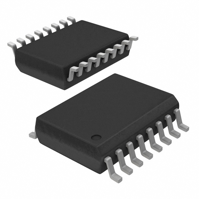
- Part No.:
- DS1023S-50/T&R
- Manufacturer:
- Analog Devices Inc./Maxim Integrated
- Category:
- Delay Lines
- Package:
- 16-SOIC (0.295", 7.50mm Width)
- Datasheet:
-
 DS1023S-50/T&R.pdf
- Description:
- IC DEL LN 256TAP 127.5NS 16SOIC
- Quantity:
- Payment:

- Shipping:

Inventory:1,722
Please send an inquiry. Send us your inquiry, and we will respond immediately.
Product details
Overview
DS1023S-50/T&R from Maxim Integrated (formerly Dallas Semiconductor) is an 8-bit programmable silicon delay line configured for 0.5 ns step resolution, 127.5 ns maximum delay in normal mode, and ±2 ns integral non-linearity. It operates from a single 5V supply, supports parallel/serial programming, and delivers precise clock phase control or pulse width modulation in test instrumentation and digital timing systems.
For engineers reviewing the DS1023S-50/T&R datasheet, DS1023S-50/T&R pinout, DS1023S-50/T&R application, or DS1023S-50/T&R equivalent, this device enables full 0–360° clock phase adjustment via on-chip reference delay compensation, supports daisy-chained serial programming, and provides dual output modes (delayed/inverted OUT and REF/PWM) controlled by MS and P/S pins.
Technical Context
The DS1023S-50/T&R implements a revised internal delay line architecture allowing input clock delays up to one full period or more, with guaranteed monotonicity across its 256-step range. Its on-chip reference delay (18–22 ns) offsets inherent step-zero delay (−2 to 22 ns), enabling true zero-relative delay measurement referenced to REF.
It supports three configurable operating modes: delay line (MS = 0), pulse width modulator (MS = 1, PWM on REF), and free-running oscillator (MS = 1 with external IN–OUT feedback). Programming is performed either in parallel (P0–P7 + LE) or serially (D/P2, CLK/P1, Q/P0), sharing pins between modes as defined by P/S polarity.
Key Specifications
| Parameter | Value and Actual Design Meaning |
|---|---|
| Delay Step Size | 0.5 ns - smallest programmable increment; enables fine-grained phase alignment in high-speed clock domains. |
| Max Delay (wrt REF) | 127.5 ns - absolute maximum delay achievable in normal mode; sufficient for sub-8 MHz clock period alignment. |
| Step Zero Delay | −2 to 22 ns - inherent propagation delay at zero programming; compensated by on-chip REF output. |
| Reference Delay | 18–22 ns - trimmed fixed delay used as timing baseline; cancels process/temperature drift of step-zero delay. |
| Integral Non-linearity | ±2 ns - max deviation from ideal linear delay vs. code; ensures predictable timing error across full range. |
| Min Input Pulse Width | 20 ns - shortest valid input pulse; supports operation up to 25 MHz clock frequency in delay mode. |
| Supply Voltage | 4.75–5.25 V - single-rail CMOS-compatible supply; eliminates need for level-shifting in 5V logic systems. |
Pinout & Package
DS1023S-50/T&R is supplied in a 16-pin 300-mil SOIC package (JEDEC MS-012AC), surface-mount compatible with standard reflow profiles and board space constraints typical in test equipment and embedded timing modules.
| Pin/Terminal | Circuit Role | Design Meaning |
|---|---|---|
| IN | Signal Input | Primary timing signal source; all delay functions referenced to rising edge. |
| OUT / OUT | Programmable Output | Delayed (MS=0) or inverted delayed (MS=1) replica of IN; used for phase-shifted clocks or oscillator feedback. |
| REF / PWM | Reference or Modulated Output | Fixed 18–22 ns reference (MS=0) or rising-edge-triggered PWM output (MS=1); enables zero-baseline measurement or duty-cycle control. |
| P0–P7 | Parallel Data Inputs | 8-bit delay value bus; P0–P2 double as serial I/O in serial mode; unused P3–P7 must be tied to VCC/GND. |
| LE | Latch Enable | Active-high control for parallel data capture; latches P0–P7 when transitioned low; must be high during serial access. |
| P/S | Programming Mode Select | Low = parallel mode; high = serial mode; polarity reversed vs. DS1020/DS1021. |
| MS | Output Mode Select | Low = delay line mode (OUT = delayed, REF = reference); high = PWM/oscillator mode (REF = PWM, OUT = inverted). |
| VCC, GND | Power Supply | Single 5V supply with decoupling recommended; CMOS inputs require defined logic levels on all unused pins. |
Key Features
| Feature | Design Value |
|---|---|
| On-chip reference delay | 18–22 ns trimmed delay used as stable baseline to cancel step-zero variation and enable true zero-relative delay calibration. |
| Configurable output modes | Three distinct system roles: precision delay line (MS=0), pulse width modulator (MS=1, PWM on REF), or free-running oscillator (MS=1 with IN–OUT loop). |
| Dual programming interfaces | Parallel (8-bit bus + LE) for fast static configuration; serial (MSB-first, daisy-chainable) for compact microcontroller control or multi-device synchronization. |
| Guaranteed monotonic delay | No delay reduction with increasing code value; ensures deterministic timing behavior critical for closed-loop phase alignment and jitter-sensitive applications. |
| Full-period+ clock delay | Supports delaying clocks beyond one full period (e.g., 127.5 ns at 25 MHz = ~3.2× period), enabling advanced skew compensation and time-interleaved sampling. |
Applications
| Automatic Test Equipment (ATE) | Digital Phase Alignment |
|---|---|
Use Scenario: Precise stimulus-response timing in boundary-scan or functional test systems where signal launch and capture must be synchronized within sub-nanosecond windows. IC Role / Device Role / Timing Role: Programmable delay element generating calibrated timing offsets between pattern generator outputs and digitizer sampling clocks. Use Value: Enables deterministic setup/hold margin verification at 25 MHz clock rates using 0.5 ns step resolution and ±2 ns linearity-critical for high-yield production testing. | Use Scenario: Aligning clock edges across multiple FPGA banks or ASIC clock domains to minimize inter-chip skew in high-speed serial link receivers. IC Role / Device Role / Timing Role: Clock phase shifter compensating for PCB trace length mismatches and package-induced delays in multi-lane SerDes subsystems. Use Value: Delivers full 0–360° phase coverage using on-chip REF compensation, eliminating need for external delay-matching components or iterative layout revisions. |
| Pulse Width Modulation Control | Free-Running Oscillator Generation |
Use Scenario: Generating variable-duty-cycle timing pulses for analog front-end calibration, LED dimming, or power converter gate drive in embedded instrumentation. IC Role / Device Role / Timing Role: Hardware-based PWM generator triggered by system clock edge, with pulse width set by 8-bit register and minimum 5 ns width guarantee. Use Value: Provides jitter-free, temperature-stable pulse widths without MCU intervention-reducing firmware overhead and improving repeatability in lab-grade equipment. | Use Scenario: Creating stable, user-adjustable clock sources for prototype validation, where crystal oscillators are unavailable or too inflexible. IC Role / Device Role / Timing Role: Inverting delay element configured as ring oscillator; output frequency determined solely by programmed delay value (e.g., 3.6–22 MHz for DS1023S-50). Use Value: Enables rapid frequency tuning via digital interface-no external components required-while maintaining monotonic frequency vs. code behavior for predictable sweep testing. |
Equivalent & Alternatives
The following parts are listed as comparable options for similar programmable delay line applications.
| Alternative Part | Technical Difference | Application Difference | Selection Advice |
|---|---|---|---|
| DS1023-50 | Same die, 16-pin DIP package; identical electrical specs and timing performance. | Through-hole mounting only; unsuitable for high-density SMT layouts or automated assembly. | Select DS1023-50 only for prototyping, legacy repair, or hand-soldered evaluation where SOIC footprint is unavailable. |
| MAX9622 | Single 5 ns step, 255-step range, 1.25 µs max delay; 3.3 V supply; no REF output or PWM mode. | Designed for lower-frequency, low-voltage systems; lacks reference-compensated zero-delay capability and dual-mode flexibility. | Choose MAX9622 only when 3.3 V operation, longer delay range, or simplified interface outweighs need for 0.5 ns resolution and REF-based calibration. |
Compared with DS1023-50 (DIP) and MAX9622 (3.3 V, coarser step), DS1023S-50/T&R uniquely combines 0.5 ns resolution, 5 V compatibility, on-chip REF compensation, and triple-mode operation in a production-ready SOIC tape-and-reel format-making it optimal for ATE timing modules and phase-critical digital systems requiring SMT scalability.
Availability
DS1023S-50/T&R is available at Aetrix Electronics and suitable for automatic test equipment, digital phase alignment, pulse width modulation control, and free-running oscillator generation requiring stable component supply, long-term lifecycle support, and consistent parametric performance across production batches.
Supply support for DS1023S-50/T&R includes scheduled delivery planning, volume procurement assistance, BOM continuity management, traceable sourcing, and lifecycle availability coordination for OEM customers, industrial embedded developers, connected-device designers, and electronics production programs.
Manufacturer
Maxim Integrated (acquired by Analog Devices in 2021) is a U.S.-based semiconductor company specializing in precision analog, mixed-signal, and high-reliability timing solutions for industrial, communications, and test equipment markets.
The DS1023 product line was designed specifically for programmable timing applications demanding sub-nanosecond resolution, monotonic delay behavior, and flexible configuration-targeting ATE, digital oscilloscopes, and high-speed data acquisition systems.
FAQ
What is the maximum clock frequency supported by DS1023S-50/T&R in delay line mode?
The DS1023S-50/T&R supports a maximum input clock frequency of 25 MHz in normal delay mode, based on its minimum input pulse width specification of 20 ns. This limit ensures accurate delay registration and avoids metastability or timing violation in the internal latch structure. Operation above 25 MHz may result in unpredictable delay values or failure to capture input transitions reliably. The DS1023S-50/T&R datasheet confirms this rating under standard test conditions (TA = 0°C to 70°C, VCC = 5V ±5%).
Does DS1023S-50/T&R support daisy-chained serial programming?
Yes, DS1023S-50/T&R supports daisy-chained serial programming: the Q/P0 pin outputs the MSB-to-LSB bitstream of the current register while new data is shifted in via D/P2, enabling cascaded configuration of multiple devices using a single serial bus. Each DS1023S-50/T&R contributes eight bits per cycle, and the total bit count equals 8 × number of devices. This feature is explicitly documented in the "CASCADING MULTIPLE DEVICES (DAISY CHAIN)" section of the DS1023S-50/T&R datasheet.
How does the REF output improve timing accuracy in DS1023S-50/T&R?
The REF output in DS1023S-50/T&R provides a fixed 18–22 ns delay that cancels step-zero variation and process/temperature drift, enabling true zero-relative delay measurement. When delay is measured between REF and OUT instead of IN and OUT, offset errors are eliminated-resulting in higher absolute accuracy and stability. The DS1023S-50/T&R datasheet states that using REF "totally removes" effects of input voltage/transition time variation and "cancels out" adverse temperature coefficients affecting step-zero delay.
Can DS1023S-50/T&R generate a free-running oscillator without external components?
Yes, DS1023S-50/T&R can generate a free-running oscillator by externally connecting the OUT pin back to the IN pin while configuring MS = 1. In this mode, the device operates as an inverting delay element forming a ring oscillator, with output frequency determined solely by the programmed delay value (e.g., 3.6–22 MHz for DS1023S-50/T&R). No external resistors or capacitors are required-the DS1023S-50/T&R datasheet confirms this functionality in the "Oscillator Configuration" table and Figure 4.
What is the minimum usable PWM pulse width from DS1023S-50/T&R's REF output?
The minimum reliable PWM pulse width from DS1023S-50/T&R's REF output is 5 ns, as specified in the "Minimum PWM Output Pulse Width" parameter. Pulse widths below 5 ns may cause degraded high-level voltage or complete loss of output due to internal response limitations. This value is confirmed across all DS1023 speed grades in the AC Electrical Characteristics tables and is independent of input frequency or supply voltage within rated conditions.
DS1023S-50/T&R Specifications
- Product attributes
- Attribute value
- Manufacturer:
- Analog Devices Inc./Maxim Integrated
- Series:
- -
- Package/Case:
- 16-SOIC (0.295", 7.50mm Width)
- Packaging:
- Tape & Reel (TR)
- Product Status:
- Obsolete
- Number of Taps/Steps:
- 256
- Function:
- 1-Shot, Programmable
- Delay to 1st Tap:
- 16.5ns
- Tap Increment:
- 500 ps
- Available Total Delays:
- 127.5ns
- Number of Independent Delays:
- 1
- Voltage - Supply:
- 4.75V ~ 5.25V
- Operating Temperature:
- 0°C ~ 70°C
- Grade:
- -
- Qualification:
- -
- Mounting Type:
- Surface Mount
- Supplier Device Package:
- 16-SOIC
DS1023S-50/T&R FAQ
1.How can I place an order for DS1023S-50/T&R through Aetrix?
Please submit a Request for Quotation (RFQ) for DS1023S-50/T&R on Aetrix. Our sales agent will provide a competitive quotation and guide you through the order confirmation once you accept the terms.
2.Are the price and stock information for DS1023S-50/T&R reliable?
The price and inventory of DS1023S-50/T&R are updated periodically and may fluctuate due to market conditions. Stock and pricing data are typically refreshed every 24 hours. Quotation validity for DS1023S-50/T&R is usually 5 days.
3.What payment methods are accepted for DS1023S-50/T&R?
We accept Wire Transfer, PayPal, Credit Card, Western Union, MoneyGram, and Escrow for DS1023S-50/T&R transactions.
Note: Certain payment methods may incur a processing fee.
4.How is shipping managed for DS1023S-50/T&R?
DS1023S-50/T&R orders can be shipped via leading logistics carriers, including DHL, UPS, FedEx, TNT, or Registered Mail.
Once your DS1023S-50/T&R order is processed, you will receive an email with the shipment details and tracking number.
Note: Tracking information may take up to 24 hours to appear. Express delivery typically takes 3–5 business days.
5.How can I obtain technical support or documentation for DS1023S-50/T&R?
For technical support, including DS1023S-50/T&R datasheets, pinout diagrams, or application guidance, please contact our engineering support team. They can provide detailed documentation and assistance for your DS1023S-50/T&R requirements.
6.How does Aetrix verify that DS1023S-50/T&R is sourced from the original manufacturer or authorized distributors?
All DS1023S-50/T&R products on Aetrix are procured from qualified distributors and authorized channels. Our dedicated quality assurance team conducts strict verification, including traceability checks and, if necessary, third-party testing. This ensures that DS1023S-50/T&R meets industry standards.
7.What is the process for return or replacement of DS1023S-50/T&R?
All DS1023S-50/T&R units undergo pre-shipment inspection (PSI). If there is an issue with DS1023S-50/T&R, returns or replacements are accepted under the following conditions:
1.Quantity discrepancies, incorrect items, or visible external defects (such as breakage or corrosion), acknowledged by Aetrix.
2.The issue is reported within 90 days of delivery.
3.The DS1023S-50/T&R part is unused and in its original packaging.
Return procedure for DS1023S-50/T&R:
1.Submit a request within 90 days.
2.Obtain a Return Material Authorization (RMA) from Aetrix.
DS1023S-50/T&R Tags
-
LTC6994CS6-1#TRMPBF
Analog Devices Inc.
-
LTC6994CDCB-1#TRMPBF
Analog Devices Inc.
-
LTC6994IS6-1#TRMPBF
Analog Devices Inc.
-
LTC6994IS6-1#TRPBF
Analog Devices Inc.
-
LTC6994IDCB-1#TRMPBF
Analog Devices Inc.
-
LTC6994IS6-2#TRMPBF
Analog Devices Inc.
-
LTC6994HS6-1#TRPBF
Analog Devices Inc.
-
LTC6994HS6-1#TRMPBF
Analog Devices Inc.
-
LTC6994HS6-2#TRMPBF
Analog Devices Inc.
-
LTC6994HDCB-2#TRMPBF
Analog Devices Inc.
-
LTC6994HDCB-1#TRMPBF
Analog Devices Inc.
-
DS1124U-25+T
Analog Devices Inc./Maxim Integrated
Tech Hub

A practical engineering guide to 3.3V and 5V logic compatibility, input thresholds, resistor dividers, translator ICs, MOSFET level shifting, I2C pull-ups, timing limits and power-sequencing risks.

The 74HC595 uses push-pull logic outputs, while the TPIC6B595 uses 50 V open-drain DMOS sinks for higher-power loads. This guide compares timing, current limits, 3.3 V interfacing, load wiring, thermal…

The 74HC595 converts serial data into eight stable parallel outputs. This guide covers pin functions, shift and storage timing, OE and MR behavior, drive-current limits, cascading, voltage compatibilit…

A technical comparison of level-sensitive latches and edge-triggered flip-flops, covering timing windows, setup and hold limits, master–slave operation, time borrowing, race-through, HDL inference and…

A D latch stores one bit while Enable controls when data can pass. This reference covers gate-level operation, truth tables, transparency, setup and hold timing, LE versus OE, common ICs and practical …

An SR latch stores one bit through cross-coupled feedback. This engineering reference covers NOR and NAND implementations, truth tables, forbidden-state recovery, gated operation, switch debouncing, fa…

Latch circuits retain one bit through feedback. This technical reference covers SR and D latches, truth tables, transparency, timing limits, latch-versus-flip-flop behavior, applications and common log…

An engineering guide to LED driver operation, constant-current and constant-voltage outputs, linear and switching topologies, dimming, IC selection, calculations, replacement compatibility, and fault c…

Operational amplifier guide covering op amp basics, feedback, ideal vs real op amps, common configurations, buffer circuits, offset, bias current, gain-bandwidth, slew rate, rail-to-rail limits and sel…

Jumper cables guide covering safe connection order, red and black clamp placement, final ground connection, cable gauge, length, clamp quality, copper vs CCA cables, jump starter comparison and battery…


