
 My Inquiry
 My Account


Analog Devices Inc./Maxim Integrated DS1088EX-133+T
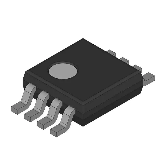
- Part No.:
- DS1088EX-133+T
- Manufacturer:
- Analog Devices Inc./Maxim Integrated
- Package:
- -
- Datasheet:
-
 DS1088EX-133+T.pdf
- Description:
- DS1088 LOW-COST FIXED-FREQUENCY
- Quantity:
- Payment:

- Shipping:

Inventory:15,000
Please send an inquiry. Send us your inquiry, and we will respond immediately.
Product details
Overview
DS1088EX-133+T from Maxim Integrated is a factory-calibrated, fixed-frequency EconOscillator™ delivering a 133MHz square-wave clock output with ±1.0% frequency tolerance over voltage and temperature, 2.7V–3.6V supply operation, and active-low power-down control. It requires no external timing components and operates across –20°C to +85°C for embedded timing in space-constrained peripherals.
For engineers reviewing the DS1088EX-133+T datasheet, DS1088EX-133+T pinout, DS1088EX-133+T application, or DS1088EX-133+T equivalent, key selection criteria include guaranteed 133MHz output stability, µSOP-8 package compatibility, power-down current ≤10µA, load capacitance support up to 50pF, and factory-trimmed frequency accuracy without calibration overhead.
Technical Context
The DS1088EX-133+T integrates a voltage-controlled oscillator (80–160MHz range) followed by a programmable prescaler (÷1, ÷2, ..., ÷256) to generate its fixed 133MHz output. Its EEPROM stores factory-set division ratio and trim settings, enabling single-output clock generation without external crystals or capacitors.
Power management is implemented via the PDN pin: asserting low disables the VCO and output within ≤7ns, reducing supply current to ≤10µA; recovery requires ≥512 internal clock cycles (~3.8µs at 133MHz) plus stabilization delay. Output duty cycle is 40–60% for fO ≥80MHz and 50% typical at 133MHz.
Key Specifications
| Parameter | Value and Actual Design Meaning |
|---|---|
| Output Frequency | 133MHz - precisely factory-programmed, no external tuning required |
| Frequency Tolerance | ±1.0% over full voltage (2.7–3.6V) and temperature (–20°C to +85°C) range - eliminates system-level recalibration |
| Supply Voltage | 2.7V to 3.6V - compatible with 3.3V logic domains and low-power embedded rails |
| Power-Down Current | ≤10µA - enables ultra-low standby power in battery-backed or energy-sensitive systems |
| Output Load Drive | CL = 15pF to 50pF - supports standard CMOS loads without external buffering |
| Duty Cycle | 40–60% at 133MHz - meets setup/hold timing margins for synchronous logic interfaces |
| Power-Up Stabilization | ~3.8µs (512 cycles @ 133MHz) - defines minimum reset release timing after VCC ramp |
Pinout & Package
DS1088EX-133+T is housed in an 8-pin µSOP package (outline 21-0036), RoHS-compliant, with exposed pad not connected. Pin 1 is OUT; pins 2 and 3 are VCC; pins 4 and 5 are GND; pin 6 is PDN (active-low); pins 7 and 8 are DNC (internally grounded, must be left unconnected).
| Pin/Terminal | Circuit Role | Design Meaning |
|---|---|---|
| 1 (OUT) | Oscillator output | CMOS-compatible 133MHz square wave; drives 15–50pF loads directly |
| 2, 3 (VCC) | Power supply | Dual VCC pins reduce IR drop and improve PSRR; require local 0.01µF + 0.1µF ceramic decoupling |
| 4, 5 (GND) | Ground reference | Dual GND pins provide low-inductance return path; must connect to solid ground plane |
| 6 (PDN) | Active-low power-down control | Pull high (≥0.7×VCC) to enable; pull low (≤0.3×VCC) to disable output and enter ≤10µA standby |
| 7, 8 (DNC) | Do-not-connect terminals | Internally tied to GND; must remain unconnected on PCB to avoid parasitic coupling |
Key Features
| Feature | Design Value |
|---|---|
| Factory-trimmed frequency | 133MHz output calibrated at wafer level - eliminates BOM cost and layout area for crystal + load caps |
| No external timing components | Self-contained oscillator core - removes risk of crystal aging, ESD sensitivity, and board-level tuning drift |
| Low-power shutdown mode | 10µA max ICCQ - enables dynamic clock gating in portable or always-on edge devices |
| Wide supply voltage range | 2.7V–3.6V operation - supports legacy 3.3V rails and newer low-voltage SoC interfaces |
| Stable duty cycle | 40–60% at 133MHz - ensures reliable sampling in DDR, USB, and PCIe clock domains |
Applications
| Printers & Copiers | POS Terminals |
|---|---|
|
Use Scenario: Synchronizing print engine motor control, image sensor readout, and USB host interface in compact office peripherals. IC Role / Device Role / Timing Role: Primary system clock source for MCU, FPGA, and peripheral bridges. Use Value: Eliminates crystal + capacitor footprint while maintaining 133MHz timing integrity across thermal cycling during high-duty-cycle operation. |
Use Scenario: Providing precise clocking for payment processing ICs, display controllers, and secure element communication in retail point-of-sale hardware. IC Role / Device Role / Timing Role: Fixed-frequency reference for cryptographic co-processors and EMV-compliant smart-card readers. Use Value: ±1.0% frequency stability ensures deterministic timing for ISO/IEC 7816-3 and contactless NFC protocols without software compensation. |
| Automotive Telematics | Cable Modems |
|
Use Scenario: Clocking GPS baseband processors and CAN-FD interface controllers in vehicle infotainment head units. IC Role / Device Role / Timing Role: Low-jitter, temperature-stable clock generator for RF front-end synchronization and data link layer timing. Use Value: Operates reliably from –20°C to +85°C with no frequency derating - avoids requalification for extended ambient ranges. |
Use Scenario: Driving DOCSIS 3.0/3.1 PHY layers and packet-processing engines in residential broadband gateways. IC Role / Device Role / Timing Role: System master clock for QAM demodulators and MAC-layer state machines. Use Value: 133MHz output meets DOCSIS spectral mask requirements while enabling direct connection to 133MHz-capable SerDes lanes. |
Equivalent & Alternatives
The following parts are listed as comparable options for similar fixed-frequency oscillator applications.
| Alternative Part | Technical Difference | Application Difference | Selection Advice |
|---|---|---|---|
| Si510-133.000M | Programmable I²C-configurable XO; ±50ppm initial accuracy; 3.3V only; 7mA active current | Requires configuration firmware; supports frequency agility but adds startup latency | Choose when field-upgradable frequency or multi-rate operation is needed |
| ABM3B-133.000MHZ-D2Y-T | 133MHz fundamental-mode quartz crystal; requires external oscillator circuit; ±20ppm tolerance; 10pF load | Higher board-level component count; sensitive to layout parasitics and aging | Choose when lowest phase noise or long-term aging stability (<±5ppm/year) is critical |
Compared with Si510-133.000M and ABM3B-133.000MHZ-D2Y-T, DS1088EX-133+T offers lowest BOM count and fastest time-to-operate, trades off configurability and ultra-fine frequency resolution for guaranteed 133MHz accuracy with zero external components and sub-4µs wake-up.
Availability
DS1088EX-133+T is available at Aetrix Electronics and suitable for printers, POS terminals, automotive telematics modules, and cable modems requiring stable component supply, consistent factory-calibrated frequency, and RoHS-compliant µSOP packaging.
Supply support for DS1088EX-133+T includes scheduled delivery planning, volume procurement assistance, BOM continuity management, traceable sourcing, and lifecycle availability coordination for OEM customers, industrial embedded developers, connected-device designers, and electronics production programs.
Manufacturer
Maxim Integrated (now part of Analog Devices) designs precision analog, mixed-signal, and timing solutions for industrial, automotive, and communications markets, with emphasis on integration and reliability.
The DS1088EX-133+T belongs to the EconOscillator™ family - engineered to replace discrete crystal oscillators in cost- and space-sensitive applications where fixed-frequency accuracy and fast enable/disable response are prioritized over programmability.
FAQ
What is the exact output frequency of DS1088EX-133+T?
The DS1088EX-133+T is factory-programmed to deliver a nominal 133.000MHz square-wave output. Measured frequency variation is bounded by ±1.0% across the full operating voltage (2.7V–3.6V) and temperature (–20°C to +85°C) range, with typical deviation under ±0.3% at 25°C and 3.3V. This value is stored in on-chip EEPROM and cannot be modified in the field.
Does DS1088EX-133+T require external capacitors or resistors?
No, DS1088EX-133+T requires no external timing components. It integrates a factory-trimmed VCO and prescaler to generate its 133MHz output. Only two ceramic decoupling capacitors (0.01µF and 0.1µF) placed near VCC/GND pins are mandatory for stable operation - no load capacitors, pull-ups, or series resistors are needed on the OUT or PDN lines.
How does the power-down function work on DS1088EX-133+T?
The DS1088EX-133+T enters power-down mode when the PDN pin is driven low (≤0.3×VCC). Output disables within ≤7ns, and supply current drops to ≤10µA. To exit, PDN must be pulled high (≥0.7×VCC); the device then waits ~3.8µs (512 internal cycles at 133MHz) before enabling the output, ensuring VCO stabilization.
What is the recommended PCB layout for DS1088EX-133+T?
Place DS1088EX-133+T close to the load it clocks. Use dual 0.01µF and 0.1µF X7R ceramic capacitors between each VCC pin and the nearest GND pin, with short, wide traces. Keep OUT trace short and away from noisy signals. Leave pins 7 and 8 (DNC) unconnected - do not route or solder them. Ensure solid ground plane beneath the µSOP body.
Is DS1088EX-133+T pin-compatible with other DS1088L variants?
Yes, DS1088EX-133+T shares the same 8-pin µSOP package (U8+1 outline), pinout, and electrical interface as all DS1088L-series devices including DS1088LU-100+, DS1088LU-66+, and DS1088LU-16+. All variants use identical VCC, GND, OUT, PDN, and DNC pin assignments - only the factory-programmed output frequency differs.
DS1088EX-133+T Specifications
- Product attributes
- Attribute value
- Manufacturer:
- Analog Devices Inc./Maxim Integrated
- Series:
- -
- Package/Case:
- -
- Packaging:
- Bulk
- Product Status:
- Active
- Programmable:
- Not Verified
- Type:
- Clock Generator
- PLL:
- No
- Input:
- -
- Output:
- -
- Number of Circuits:
- 1
- Ratio - Input:Output:
- 1:1
- Differential - Input:Output:
- No/No
- Frequency - Max:
- 133MHz
- Divider/Multiplier:
- Yes/No
- Voltage - Supply:
- 2.85V ~ 3.63V
- Operating Temperature:
- -40°C ~ 95°C (TA)
- Mounting Type:
- -
- Grade:
- -
- Qualification:
- -
- Supplier Device Package:
- -
DS1088EX-133+T FAQ
1.How can I place an order for DS1088EX-133+T through Aetrix?
Please submit a Request for Quotation (RFQ) for DS1088EX-133+T on Aetrix. Our sales agent will provide a competitive quotation and guide you through the order confirmation once you accept the terms.
2.Are the price and stock information for DS1088EX-133+T reliable?
The price and inventory of DS1088EX-133+T are updated periodically and may fluctuate due to market conditions. Stock and pricing data are typically refreshed every 24 hours. Quotation validity for DS1088EX-133+T is usually 5 days.
3.What payment methods are accepted for DS1088EX-133+T?
We accept Wire Transfer, PayPal, Credit Card, Western Union, MoneyGram, and Escrow for DS1088EX-133+T transactions.
Note: Certain payment methods may incur a processing fee.
4.How is shipping managed for DS1088EX-133+T?
DS1088EX-133+T orders can be shipped via leading logistics carriers, including DHL, UPS, FedEx, TNT, or Registered Mail.
Once your DS1088EX-133+T order is processed, you will receive an email with the shipment details and tracking number.
Note: Tracking information may take up to 24 hours to appear. Express delivery typically takes 3–5 business days.
5.How can I obtain technical support or documentation for DS1088EX-133+T?
For technical support, including DS1088EX-133+T datasheets, pinout diagrams, or application guidance, please contact our engineering support team. They can provide detailed documentation and assistance for your DS1088EX-133+T requirements.
6.How does Aetrix verify that DS1088EX-133+T is sourced from the original manufacturer or authorized distributors?
All DS1088EX-133+T products on Aetrix are procured from qualified distributors and authorized channels. Our dedicated quality assurance team conducts strict verification, including traceability checks and, if necessary, third-party testing. This ensures that DS1088EX-133+T meets industry standards.
7.What is the process for return or replacement of DS1088EX-133+T?
All DS1088EX-133+T units undergo pre-shipment inspection (PSI). If there is an issue with DS1088EX-133+T, returns or replacements are accepted under the following conditions:
1.Quantity discrepancies, incorrect items, or visible external defects (such as breakage or corrosion), acknowledged by Aetrix.
2.The issue is reported within 90 days of delivery.
3.The DS1088EX-133+T part is unused and in its original packaging.
Return procedure for DS1088EX-133+T:
1.Submit a request within 90 days.
2.Obtain a Return Material Authorization (RMA) from Aetrix.
DS1088EX-133+T Tags

-
CD74HCT4046AM96
Texas Instruments

-
MC14046BDWR2G
onsemi

-
501MILFT
Renesas
-
CD74HC7046AM
Texas Instruments

-
CDCVF2505PWR
Texas Instruments

-
RC19004A100GNL#KB0
Renesas

-
SI5351A-B-GTR
Skyworks Solutions Inc.

-
CY2305SXI-1T
Infineon Technologies
-
570BILFT
Renesas

-
CDCE913PWR
Texas Instruments
-
CY2305SXI-1HT
Infineon Technologies

-
DS1086LU+T
Analog Devices Inc./Maxim Integrated
Tech Hub

A practical engineering guide to 3.3V and 5V logic compatibility, input thresholds, resistor dividers, translator ICs, MOSFET level shifting, I2C pull-ups, timing limits and power-sequencing risks.

The 74HC595 uses push-pull logic outputs, while the TPIC6B595 uses 50 V open-drain DMOS sinks for higher-power loads. This guide compares timing, current limits, 3.3 V interfacing, load wiring, thermal…

The 74HC595 converts serial data into eight stable parallel outputs. This guide covers pin functions, shift and storage timing, OE and MR behavior, drive-current limits, cascading, voltage compatibilit…

A technical comparison of level-sensitive latches and edge-triggered flip-flops, covering timing windows, setup and hold limits, master–slave operation, time borrowing, race-through, HDL inference and…

A D latch stores one bit while Enable controls when data can pass. This reference covers gate-level operation, truth tables, transparency, setup and hold timing, LE versus OE, common ICs and practical …

An SR latch stores one bit through cross-coupled feedback. This engineering reference covers NOR and NAND implementations, truth tables, forbidden-state recovery, gated operation, switch debouncing, fa…

Latch circuits retain one bit through feedback. This technical reference covers SR and D latches, truth tables, transparency, timing limits, latch-versus-flip-flop behavior, applications and common log…

An engineering guide to LED driver operation, constant-current and constant-voltage outputs, linear and switching topologies, dimming, IC selection, calculations, replacement compatibility, and fault c…

Operational amplifier guide covering op amp basics, feedback, ideal vs real op amps, common configurations, buffer circuits, offset, bias current, gain-bandwidth, slew rate, rail-to-rail limits and sel…

Jumper cables guide covering safe connection order, red and black clamp placement, final ground connection, cable gauge, length, clamp quality, copper vs CCA cables, jump starter comparison and battery…


