
 My Inquiry
 My Account


Analog Devices Inc./Maxim Integrated DS1110LE-100+
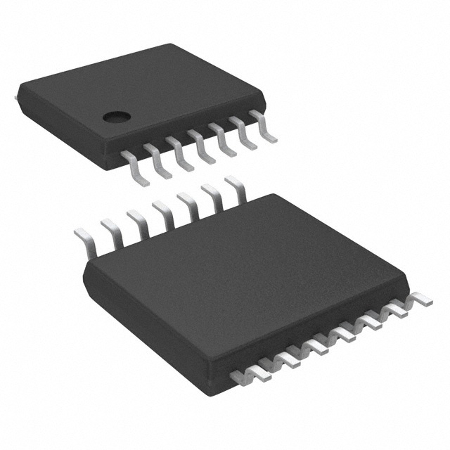
- Part No.:
- DS1110LE-100+
- Manufacturer:
- Analog Devices Inc./Maxim Integrated
- Category:
- Delay Lines
- Package:
- 14-TSSOP (0.173", 4.40mm Width)
- Datasheet:
-
 DS1110LE-100+.pdf
- Description:
- IC DELAY LN 10TAP 100NS 14TSSOP
- Quantity:
- Payment:

- Shipping:

Inventory:1,922
Please send an inquiry. Send us your inquiry, and we will respond immediately.
Product details
Overview
DS1110LE-100+ from Maxim Integrated is a 3V, 10-tap all-silicon delay line with total delay of 100ns, ±5% or ±2ns accuracy at 3.3V/+25°C, 2.7V–3.6V supply range, and TTL/CMOS-compatible outputs-used for precise timing alignment in high-speed digital test and medical synchronization circuits.
For engineers reviewing the DS1110LE-100+ datasheet, DS1110LE-100+ pinout, DS1110LE-100+ application, or DS1110LE-100+ equivalent, key selection factors include tap spacing (10ns), leading/trailing-edge matching, industrial temperature range (−40°C to +85°C), TSSOP-14 package compatibility, and load drive capability (10 × 74LS loads).
Technical Context
The DS1110LE-100+ implements a monolithic silicon delay architecture with fixed, equally spaced taps-each output reproduces the input logic state after a deterministic delay, with identical propagation characteristics for rising and falling edges. It operates without external clocks or configuration registers, relying solely on analog delay-line physics.
Delay stability is maintained across voltage (2.7V–3.6V) and temperature (−40°C to +85°C) via process-compensated design; all taps track unidirectionally-e.g., if Tap 1 slows, all others slow proportionally. Input pulse width minimum is 10ns, and output loading is specified at 15pF + 450Ω per tap.
Key Specifications
| Parameter | Value and Actual Design Meaning |
|---|---|
| Total Delay | 100ns nominal; defines fixed latency from IN to TAP10, enabling precise signal skew correction. |
| Tap Spacing | 10ns per tap; provides 10 discrete, equally spaced delays (TAP1 = 10ns, TAP2 = 20ns, ..., TAP10 = 100ns). |
| Delay Accuracy | ±5% or ±2ns (whichever greater) at 3.3V/+25°C; ensures predictable timing margin in synchronous systems. |
| Supply Range | 2.7V to 3.6V; supports modern low-voltage logic domains while maintaining full delay specification. |
| Operating Temp | −40°C to +85°C; qualified for industrial-grade embedded instrumentation and automated test equipment. |
| Output Drive | 12mA sink / −1mA source at VCC = 2.7V; sufficient to directly interface with 10 × 74LS loads without buffering. |
| Input Capacitance | 5–10pF typical; minimizes signal reflection and loading on high-speed source drivers. |
Pinout & Package
DS1110LE-100+ is housed in a 14-pin TSSOP (173mil body width), RoHS-compliant, vapor-phase and IR solderable package with 0.65mm lead pitch.
| Pin/Terminal | Circuit Role | Design Meaning |
|---|---|---|
| 1 | IN | Single-ended CMOS/TTL input; accepts 0–3.3V logic with 5–10pF capacitance. |
| 2 | N.C. | No internal connection; must be left floating or grounded per layout best practice. |
| 3–12 (10 pins) | TAP1–TAP10 | Delay outputs; TAP1 = 10ns, TAP2 = 20ns, ..., TAP10 = 100ns; each drives 10 × 74LS loads. |
| 13 | GND | Digital ground reference; requires low-impedance PCB plane for noise immunity. |
| 14 | VCC | Power supply input; decoupling capacitor (0.1µF) required within 5mm of pin. |
Key Features
| Feature | Design Value |
|---|---|
| All-silicon construction | Eliminates quartz or LC-based drift; delivers stable delay over time, temperature, and voltage without calibration. |
| Leading- and trailing-edge matching | Identical tPLH and tPHL tolerances ensure symmetrical pulse width preservation across all taps. |
| 14-pin TSSOP packaging | Enables high-density PCB layouts compatible with standard SMT reflow processes (IPC/JEDEC J-STD-020A). |
| Low-power CMOS operation | Typical ICC = 40–150mA depending on input frequency; reduces thermal load in multi-channel timing modules. |
| TTL/CMOS input compatibility | Accepts VIH ≥ 2.2V and VIL ≤ 0.8V-interoperable with legacy 5V logic via level-shifting or direct 3.3V system integration. |
Applications
| Communications Equipment | Medical Imaging Systems |
|---|---|
Use Scenario: Aligning parallel data lanes in high-speed serial-to-parallel conversion for optical transceivers. IC Role / Device Role / Timing Role: Fixed-latency skew compensator between clock and data paths to meet setup/hold windows. Use Value: 10ns tap resolution enables sub-cycle alignment of 100MHz+ interfaces without FPGA-based delay tuning. | Use Scenario: Synchronizing ultrasound echo sampling clocks with transmit pulse generation in portable imaging units. IC Role / Device Role / Timing Role: Deterministic delay element ensuring precise echo-gating window placement relative to excitation pulse. Use Value: ±2ns absolute accuracy at 3.3V guarantees consistent time-of-flight measurement across battery voltage variation. |
| Automated Test Equipment (ATE) | PC Peripheral Timing Control |
Use Scenario: Generating calibrated strobe delays for boundary-scan test pattern capture in JTAG chains. IC Role / Device Role / Timing Role: Tap-selectable trigger generator providing repeatable, jitter-free edge offsets for DUT stimulus timing. Use Value: Unidirectional tap tracking ensures all delay channels shift coherently under thermal stress-critical for multi-site test repeatability. | Use Scenario: Compensating for trace-length mismatch between USB 2.0 PHY clock and data lines on motherboard routing. IC Role / Device Role / Timing Role: Passive delay buffer inserted in clock path to equalize propagation to differential receivers. Use Value: 100ns total delay matches typical 15cm FR4 trace skew, eliminating need for length-matching PCB layout. |
Equivalent & Alternatives
The following parts are listed as comparable options for similar fixed-delay line applications.
| Alternative Part | Technical Difference | Application Difference | Selection Advice |
|---|---|---|---|
| DS1023S-100+ (Maxim) | 5-tap, 100ns total delay; same 14-pin TSSOP but fewer taps; ±3% accuracy at 5V. | Designed for 5V systems; lacks trailing-edge matching spec; not rated for −40°C operation. | Select only for legacy 5V designs where tap count and industrial temp are non-critical. |
| MC100EP195DG (ON Semiconductor) | 10-tap ECL delay line; 3.3V supply; ±10% delay tolerance; differential PECL outputs. | Requires ECL-level signaling and termination; higher power; unsuitable for single-ended CMOS environments. | Choose only when interfacing with high-speed differential logic and jitter-sensitive RF sampling clocks. |
Compared with DS1023S-100+ and MC100EP195DG, the DS1110LE-100+ uniquely combines 10-tap granularity, single-ended TTL/CMOS I/O, ±2ns absolute accuracy, and industrial temperature rating in a drop-in 14-pin TSSOP-making it optimal for cost-sensitive, mixed-signal embedded timing where precision and compatibility are jointly required.
Availability
DS1110LE-100+ is available at Aetrix Electronics and suitable for communications infrastructure, medical diagnostics, and automated test equipment requiring stable component supply, long-term lifecycle support, and guaranteed traceable sourcing.
Supply support for DS1110LE-100+ includes scheduled delivery planning, volume procurement assistance, BOM continuity management, traceable sourcing, and lifecycle availability coordination for OEM customers, industrial embedded developers, connected-device designers, and electronics production programs.
Manufacturer
Maxim Integrated (now part of Analog Devices) designs precision analog, mixed-signal, and timing ICs for industrial, medical, and communications applications-with emphasis on reliability, low power, and high integration.
The DS1110L series was developed specifically for deterministic, low-jitter signal delay in digital test, imaging, and synchronization systems-replacing discrete RC networks and programmable logic with a calibrated, monolithic silicon solution.
FAQ
What is the exact delay value for each tap on the DS1110LE-100+?
The DS1110LE-100+ provides 10 equally spaced taps with 10ns increments: TAP1 = 10ns, TAP2 = 20ns, TAP3 = 30ns, TAP4 = 40ns, TAP5 = 50ns, TAP6 = 60ns, TAP7 = 70ns, TAP8 = 80ns, TAP9 = 90ns, and TAP10 = 100ns. These values are specified at 3.3V and +25°C, with tolerance of ±5% or ±2ns (whichever is greater). The DS1110LE-100+ maintains proportional spacing across its full operating temperature and voltage range.
Does the DS1110LE-100+ support both rising- and falling-edge delay accuracy?
Yes, the DS1110LE-100+ guarantees matched leading-edge (tPLH) and trailing-edge (tPHL) delay accuracy-both specified under identical conditions (±5% or ±2ns at 3.3V/+25°C). This ensures preserved pulse width across all taps, critical for applications like gated sampling or clock deskewing where duty cycle integrity matters. The DS1110LE-100+ achieves this via symmetric internal delay-path design, not post-processing or trimming.
Can the DS1110LE-100+ operate from a 2.5V supply?
No, the DS1110LE-100+ is characterized and specified only for 2.7V to 3.6V operation. At 2.5V, timing parameters-including delay accuracy, output drive strength, and input threshold levels-are not guaranteed and may fall outside datasheet limits. Operation below 2.7V risks increased delay variation, reduced noise margin, and potential functional failure. The DS1110LE-100+ must be powered within its validated supply range to ensure compliance with its ±2ns accuracy specification.
Is the DS1110LE-100+ pin-compatible with other DS1110L variants like DS1110LE-200+?
Yes, all DS1110L variants-including DS1110LE-100+, DS1110LE-200+, and DS1110LE-500+-share identical 14-pin TSSOP packaging and pinout. The only difference is total delay (and thus tap spacing), which is factory-trimmed during production. No PCB layout change is needed when substituting between DS1110L variants, provided the application can accommodate the new delay profile and associated timing margins.
What is the maximum recommended input frequency for the DS1110LE-100+?
The DS1110LE-100+ does not specify a maximum input frequency, but imposes a minimum input pulse width (tWI) of 10ns and minimum period of 2×tWI (20ns), implying an effective upper limit of 50MHz for reliable delay fidelity. At higher frequencies, delay accuracy degrades due to input rise/fall time effects and capacitive loading. The DS1110LE-100+'s active current increases linearly with frequency-up to ~150mA at 50MHz with 15pF load per tap-so thermal design must account for this.
DS1110LE-100+ Specifications
- Product attributes
- Attribute value
- Manufacturer:
- Analog Devices Inc./Maxim Integrated
- Series:
- -
- Package/Case:
- 14-TSSOP (0.173", 4.40mm Width)
- Packaging:
- Tube
- Product Status:
- Active
- Number of Taps/Steps:
- 10
- Function:
- Nonprogrammable
- Delay to 1st Tap:
- 10ns
- Tap Increment:
- 10 ns
- Available Total Delays:
- 100ns
- Number of Independent Delays:
- 1
- Voltage - Supply:
- 2.7V ~ 3.6V
- Operating Temperature:
- -40°C ~ 85°C
- Grade:
- -
- Qualification:
- -
- Mounting Type:
- Surface Mount
- Supplier Device Package:
- 14-TSSOP
DS1110LE-100+ FAQ
1.How can I place an order for DS1110LE-100+ through Aetrix?
Please submit a Request for Quotation (RFQ) for DS1110LE-100+ on Aetrix. Our sales agent will provide a competitive quotation and guide you through the order confirmation once you accept the terms.
2.Are the price and stock information for DS1110LE-100+ reliable?
The price and inventory of DS1110LE-100+ are updated periodically and may fluctuate due to market conditions. Stock and pricing data are typically refreshed every 24 hours. Quotation validity for DS1110LE-100+ is usually 5 days.
3.What payment methods are accepted for DS1110LE-100+?
We accept Wire Transfer, PayPal, Credit Card, Western Union, MoneyGram, and Escrow for DS1110LE-100+ transactions.
Note: Certain payment methods may incur a processing fee.
4.How is shipping managed for DS1110LE-100+?
DS1110LE-100+ orders can be shipped via leading logistics carriers, including DHL, UPS, FedEx, TNT, or Registered Mail.
Once your DS1110LE-100+ order is processed, you will receive an email with the shipment details and tracking number.
Note: Tracking information may take up to 24 hours to appear. Express delivery typically takes 3–5 business days.
5.How can I obtain technical support or documentation for DS1110LE-100+?
For technical support, including DS1110LE-100+ datasheets, pinout diagrams, or application guidance, please contact our engineering support team. They can provide detailed documentation and assistance for your DS1110LE-100+ requirements.
6.How does Aetrix verify that DS1110LE-100+ is sourced from the original manufacturer or authorized distributors?
All DS1110LE-100+ products on Aetrix are procured from qualified distributors and authorized channels. Our dedicated quality assurance team conducts strict verification, including traceability checks and, if necessary, third-party testing. This ensures that DS1110LE-100+ meets industry standards.
7.What is the process for return or replacement of DS1110LE-100+?
All DS1110LE-100+ units undergo pre-shipment inspection (PSI). If there is an issue with DS1110LE-100+, returns or replacements are accepted under the following conditions:
1.Quantity discrepancies, incorrect items, or visible external defects (such as breakage or corrosion), acknowledged by Aetrix.
2.The issue is reported within 90 days of delivery.
3.The DS1110LE-100+ part is unused and in its original packaging.
Return procedure for DS1110LE-100+:
1.Submit a request within 90 days.
2.Obtain a Return Material Authorization (RMA) from Aetrix.
DS1110LE-100+ Tags
-
LTC6994CS6-1#TRMPBF
Analog Devices Inc.
-
LTC6994CDCB-1#TRMPBF
Analog Devices Inc.
-
LTC6994IS6-1#TRMPBF
Analog Devices Inc.
-
LTC6994IS6-1#TRPBF
Analog Devices Inc.
-
LTC6994IDCB-1#TRMPBF
Analog Devices Inc.
-
LTC6994IS6-2#TRMPBF
Analog Devices Inc.
-
LTC6994HS6-1#TRPBF
Analog Devices Inc.
-
LTC6994HS6-1#TRMPBF
Analog Devices Inc.
-
LTC6994HS6-2#TRMPBF
Analog Devices Inc.
-
LTC6994HDCB-2#TRMPBF
Analog Devices Inc.
-
LTC6994HDCB-1#TRMPBF
Analog Devices Inc.
-
DS1124U-25+T
Analog Devices Inc./Maxim Integrated
Tech Hub

A practical engineering guide to 3.3V and 5V logic compatibility, input thresholds, resistor dividers, translator ICs, MOSFET level shifting, I2C pull-ups, timing limits and power-sequencing risks.

The 74HC595 uses push-pull logic outputs, while the TPIC6B595 uses 50 V open-drain DMOS sinks for higher-power loads. This guide compares timing, current limits, 3.3 V interfacing, load wiring, thermal…

The 74HC595 converts serial data into eight stable parallel outputs. This guide covers pin functions, shift and storage timing, OE and MR behavior, drive-current limits, cascading, voltage compatibilit…

A technical comparison of level-sensitive latches and edge-triggered flip-flops, covering timing windows, setup and hold limits, master–slave operation, time borrowing, race-through, HDL inference and…

A D latch stores one bit while Enable controls when data can pass. This reference covers gate-level operation, truth tables, transparency, setup and hold timing, LE versus OE, common ICs and practical …

An SR latch stores one bit through cross-coupled feedback. This engineering reference covers NOR and NAND implementations, truth tables, forbidden-state recovery, gated operation, switch debouncing, fa…

Latch circuits retain one bit through feedback. This technical reference covers SR and D latches, truth tables, transparency, timing limits, latch-versus-flip-flop behavior, applications and common log…

An engineering guide to LED driver operation, constant-current and constant-voltage outputs, linear and switching topologies, dimming, IC selection, calculations, replacement compatibility, and fault c…

Operational amplifier guide covering op amp basics, feedback, ideal vs real op amps, common configurations, buffer circuits, offset, bias current, gain-bandwidth, slew rate, rail-to-rail limits and sel…

Jumper cables guide covering safe connection order, red and black clamp placement, final ground connection, cable gauge, length, clamp quality, copper vs CCA cables, jump starter comparison and battery…


