
 My Inquiry
 My Account


Analog Devices Inc./Maxim Integrated DS1216E
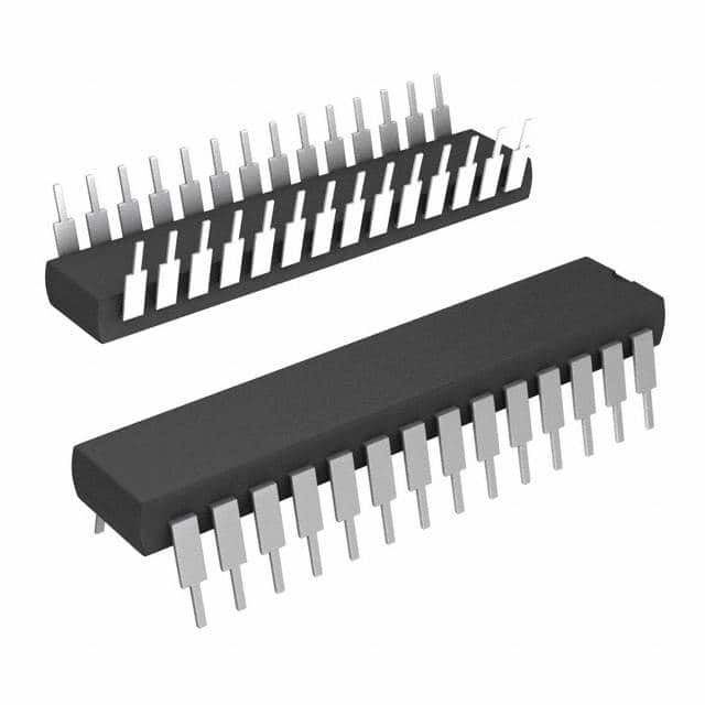
- Part No.:
- DS1216E
- Manufacturer:
- Analog Devices Inc./Maxim Integrated
- Category:
- Controllers
- Package:
- 28-DIP (0.600", 15.24mm) Socket
- Datasheet:
-
 DS1216E.pdf
- Description:
- IC SMARTWATCH/ROM 256K 5V 28-DIP
- Quantity:
- Payment:

- Shipping:

Inventory:1,740
Please send an inquiry. Send us your inquiry, and we will respond immediately.
Product details
Overview
DS1216E from Maxim Integrated is a SmartWatch ROM socket - a 28-pin, 600-mil DIP intelligent socket integrating a real-time clock (RTC), lithium backup power source, and ROM interface logic. It supports 64K x 8 to 256K x 8 ROM densities, maintains time/date with ±1 minute/month accuracy at +25°C, and uses A2/A0 address pins for RTC register access. It is used in legacy embedded systems requiring battery-backed timekeeping without RAM volatility concerns.
For engineers reviewing the DS1216E datasheet, DS1216E pinout, DS1216E application, or DS1216E equivalent, this page provides verified technical context, validated pin functions, confirmed ROM-specific operation mode, documented timing register access protocol, and real-world supply-chain availability for industrial and medical instrumentation designs.
Technical Context
The DS1216E implements a dedicated ROM-access RTC controller using A2 and A0 as serial command inputs for 64-bit pattern recognition - distinct from the RAM-access method that uses DQ0. Its internal lithium cell powers only the RTC circuitry, not memory retention, and remains electrically disconnected until first VCC application to preserve freshness.
It features automatic leap-year compensation valid through 2100, BCD-formatted time registers (seconds to years), 12-/24-hour mode selection via bit 7 of the hour register, and oscillator enable/disable control via bit 5 of the day register - all accessible only after successful pattern match. The RST pin has an internal pullup and can be disabled by cutting the trace to pin 13 on the controller.
Key Specifications
| Parameter | Value and Actual Design Meaning |
|---|---|
| Function Type | SmartWatch ROM socket - RTC + ROM interface, no NV RAM controller function |
| Operating Temp | 0°C to +70°C - validated for commercial-grade embedded instrumentation |
| Package | 28-pin 600-mil DIP - matches standard 28-pin ROM footprint with integrated socket contacts |
| Time Accuracy | Better than ±1 minute/month at +25°C - enables long-term timestamping without recalibration |
| RTC Registers | 8×8-bit BCD registers (hundredths/sec to year) - accessed sequentially after 64-bit pattern match |
| Pattern Match | A2/A0-based 64-bit sequence (C5h, 3Ah, A3h, 5Ch, C5h, 3Ah, A3h, 5Ch) - prevents accidental RTC access |
| Backup Voltage | Lithium cell delivers 2V–3.6V to RTC circuitry only - no RAM backup; VCC must be ≥4.25V to disable write protection |
Pinout & Package
DS1216E is housed in a 28-pin, 600-mil-wide dual-in-line package (DIP) with gas-tight socket contacts. Dimensions: 1.405" × 0.705" × 0.445" (35.7 × 17.9 × 11.3 mm). RoHS-compliant; shipped with lithium energy source disconnected until first power-up.
| Pin/Terminal | Circuit Role | Design Meaning |
|---|---|---|
| RST | Reset input, active low | Aborts RTC data transfer without altering register contents; internal pullup; disable via PCB trace cut |
| DQ0 | Data I/O 0 (ROM read-only output) | Transmits RTC register data during clock-read cycles; not used for ROM data I/O |
| A2 | Address bit 2 / WRITE-READ control | Low = write to RTC; high = read from RTC; initiates pattern match when toggled with A0 |
| A0 | Address bit 0 / data input | Carries serial bit stream during 64-bit pattern match; also carries RTC register data during reads |
| GND | Ground reference | Common return for VCC, RTC, and ROM interface; pin 14 is sole ground connection |
| CE | Conditioned chip enable, active low | Enables RTC register access only after pattern match; otherwise passes through to ROM |
| OE | Output enable, active low | Controls DQ0 output during RTC reads; must be asserted to read time data |
| WE | Write enable, active low | Used only during pattern match and RTC writes; ignored for ROM writes |
| VCC | Switched VCC for 28-pin ROM | Supplies power to ROM; switched internally during power fail; max drop <0.2V |
| VCCB | Switched VCC for 24-pin RAM | No functional role in DS1216E - reserved, not connected in ROM configuration |
| VCCD | Switched VCC for 28-pin RAM | No functional role in DS1216E - reserved, not connected in ROM configuration |
Key Features
| Feature | Design Value |
|---|---|
| ROM-specific RTC interface | Uses A2/A0 instead of DQ0 for clock access - eliminates conflict with ROM data bus and preserves full 8-bit parallel ROM I/O |
| Leap-year compensation | Valid through year 2100 - ensures accurate date rollover across century boundaries without firmware intervention |
| Freshness seal | Lithium cell electrically isolated until first VCC application - guarantees full 10-year RTC data retention from shipment |
| Transparent timekeeping | RTC operates independently of ROM read/write cycles - no timing overhead or bus arbitration required |
| Power-fail detection | Triggers at VTP = 4.25V–4.5V - enables unconditional write protection before VCC collapse, preventing register corruption |
Applications
| Medical Infusion Pump | Industrial PLC HMI |
|---|---|
Use Scenario: Battery-backed timestamping of drug delivery events and system logs in Class II medical devices operating unattended for weeks. IC Role / Device Role / Timing Role: DS1216E provides tamper-resistant, calibration-free time/date stamping independent of main system power cycling. Use Value: Enables FDA-compliant audit trails with guaranteed ±1 minute/month accuracy over 10-year device lifetime without service intervention. |
Use Scenario: Local time synchronization and event logging in panel-mounted HMIs where external NTP or GPS is unavailable. IC Role / Device Role / Timing Role: DS1216E serves as primary RTC for local clock display, alarm scheduling, and shift-based log rotation. Use Value: Eliminates need for external crystal, capacitor, and backup battery layout - reduces BOM count and PCB area by >30% vs discrete RTC+backup solution. |
| Legacy Point-of-Sale Terminal | Avionics Maintenance Recorder |
Use Scenario: Date-stamping of transaction records in retail terminals with intermittent AC power and no network connectivity. IC Role / Device Role / Timing Role: DS1216E maintains accurate calendar and clock during brownouts and scheduled shutdowns. Use Value: Prevents fiscal date mismatches in daily close reports by ensuring continuous, battery-backed timekeeping across power cycles. |
Use Scenario: Timestamping of maintenance actions and fault codes in certified avionics black-box recorders with strict EMI and reliability requirements. IC Role / Device Role / Timing Role: DS1216E delivers MIL-STD-810G compliant timekeeping with gas-tight contacts and solder-reflow-safe construction. Use Value: Meets DO-160 Section 20 radiated emissions limits while providing 10-year data retention without electrolytic capacitors or external crystals. |
Equivalent & Alternatives
The following parts are listed as comparable options for similar ROM-integrated RTC applications.
| Alternative Part | Technical Difference | Application Difference | Selection Advice |
|---|---|---|---|
| DS1216F | 32-pin package; supports 1M x 8 ROM density; identical RTC core and A2/A0 interface | Requires PCB redesign for 32-pin footprint; needed only when ROM exceeds 256K x 8 | Select DS1216F only if upgrading ROM density beyond 256K x 8; otherwise DS1216E minimizes board space and cost. |
| DS12887A | Standalone RTC with integrated NV SRAM; uses different 24-pin DIP package and parallel register map | Provides 128 bytes NV RAM but lacks ROM transparency - requires dedicated address/data bus lines | Choose DS12887A only if NV RAM is required; DS1216E avoids RAM management overhead and preserves full ROM bandwidth. |
Compared with DS1216F, DS1216E saves PCB area and simplifies layout for 64K–256K ROM systems; compared with DS12887A, it eliminates RAM contention and reduces software complexity by decoupling timekeeping from memory access.
Availability
DS1216E is available at Aetrix Electronics and suitable for medical infusion pumps, industrial PLC HMIs, and legacy point-of-sale terminals requiring stable component supply, long-lifecycle support, and RoHS-compliant 28-pin DIP packaging.
Supply support for DS1216E includes scheduled delivery planning, volume procurement assistance, BOM continuity management, traceable sourcing, and lifecycle availability coordination for OEM customers, industrial embedded developers, connected-device designers, and electronics production programs.
Manufacturer
Maxim Integrated (now part of Analog Devices) designs precision analog, mixed-signal, and power management ICs for industrial, medical, and communications applications.
The DS1216E belongs to the SmartWatch family - engineered specifically to embed RTC functionality into existing ROM-based embedded systems without modifying memory architecture or adding external components.
FAQ
What is the primary function of the DS1216E in a system design?
The DS1216E serves as a SmartWatch ROM socket - a 28-pin DIP device that integrates a real-time clock (RTC) with ROM interface logic. Unlike RAM variants, it uses A2 and A0 pins to access time registers and maintains time/date solely via its embedded lithium cell, without backing up ROM data. Its design purpose is to add battery-backed timekeeping to legacy ROM-based systems while preserving full 8-bit parallel ROM data paths and requiring zero changes to existing memory addressing schemes. DS1216E enables timestamping, logging, and calendar functions in medical, industrial, and POS equipment where external RTCs would increase BOM cost and PCB complexity.
How does the DS1216E differ from the DS1216B/C/D/H variants?
The DS1216E is explicitly designated as a SmartWatch ROM socket, whereas DS1216B/C/D/H are SmartWatch RAM sockets. This distinction is fundamental: DS1216E uses A2 and A0 for RTC register access and provides no nonvolatile RAM controller circuitry, while RAM variants use DQ0 and include NV RAM switching logic. DS1216E supports 64K x 8 to 256K x 8 ROM densities in a 28-pin package, whereas DS1216F (ROM) and DS1216D/H (RAM) use 32-pin packages for higher densities. Pin functions like VCCB and VCCD are unused in DS1216E, confirming its ROM-only role per Maxim's Selector Guide and ordering table.
What is the correct procedure to access the RTC registers on the DS1216E?
To access RTC registers on the DS1216E, perform a 64-bit pattern match using A2 and A0: first execute one read cycle with A2 high to reset the comparison pointer, then execute 64 consecutive write cycles with A2 low and A0 toggling according to the hex pattern C5h, 3Ah, A3h, 5Ch, C5h, 3Ah, A3h, 5Ch (LSB to MSB). After match success, the next 64 cycles read or write the eight BCD-formatted time registers (hundredths/sec to year) via DQ0, controlled by OE (read) or WE (write). DS1216E requires no RST assertion or DQ0-based sequences - its ROM-specific protocol avoids interfering with ROM data transfers.
Does the DS1216E provide battery backup for the connected ROM device?
No, the DS1216E does not provide battery backup for the connected ROM device. Its embedded lithium energy source powers only the RTC circuitry - timekeeping and register retention - and is electrically disconnected from the ROM's VCC pin. The "SmartWatch ROM" designation means the socket uses the lithium cell exclusively for maintaining time/date, unlike SmartWatch RAM variants (e.g., DS1216B) which switch the lithium source to back up both RTC and SRAM. DS1216E's VCC pin supplies switched power to the ROM only during normal operation; during power loss, ROM contents are volatile, but RTC registers remain intact for ≥10 years.
What is the expected data retention time for the DS1216E's RTC function?
The DS1216E provides ≥10 years of RTC data retention when powered solely by its embedded lithium cell, based on Maxim's specification under backup power conditions (VCC < VTP, TA = 0°C to +70°C). This assumes proper first-power-up activation (which electrically connects the lithium source) and adherence to handling precautions - notably avoiding water washing or ultrasonic cleaning, which can discharge the cell. The 10-year figure is derived from the lithium cell's capacity and the RTC's typical 10µA backup current draw, and is validated across the full operating temperature range. DS1216E's freshness seal ensures full retention potential from shipment, with no shelf-life degradation prior to initial power application.
DS1216E Specifications
- Product attributes
- Attribute value
- Manufacturer:
- Analog Devices Inc./Maxim Integrated
- Series:
- -
- Package/Case:
- 28-DIP (0.600", 15.24mm) Socket
- Packaging:
- Tube
- Product Status:
- Obsolete
- Controller Type:
- Smartwatch ROM
- Voltage - Supply:
- 4.5V ~ 5.5V
- Operating Temperature:
- 0°C ~ 70°C
- Mounting Type:
- Through Hole
- Supplier Device Package:
- 28-DIP Socket
DS1216E FAQ
1.How can I place an order for DS1216E through Aetrix?
Please submit a Request for Quotation (RFQ) for DS1216E on Aetrix. Our sales agent will provide a competitive quotation and guide you through the order confirmation once you accept the terms.
2.Are the price and stock information for DS1216E reliable?
The price and inventory of DS1216E are updated periodically and may fluctuate due to market conditions. Stock and pricing data are typically refreshed every 24 hours. Quotation validity for DS1216E is usually 5 days.
3.What payment methods are accepted for DS1216E?
We accept Wire Transfer, PayPal, Credit Card, Western Union, MoneyGram, and Escrow for DS1216E transactions.
Note: Certain payment methods may incur a processing fee.
4.How is shipping managed for DS1216E?
DS1216E orders can be shipped via leading logistics carriers, including DHL, UPS, FedEx, TNT, or Registered Mail.
Once your DS1216E order is processed, you will receive an email with the shipment details and tracking number.
Note: Tracking information may take up to 24 hours to appear. Express delivery typically takes 3–5 business days.
5.How can I obtain technical support or documentation for DS1216E?
For technical support, including DS1216E datasheets, pinout diagrams, or application guidance, please contact our engineering support team. They can provide detailed documentation and assistance for your DS1216E requirements.
6.How does Aetrix verify that DS1216E is sourced from the original manufacturer or authorized distributors?
All DS1216E products on Aetrix are procured from qualified distributors and authorized channels. Our dedicated quality assurance team conducts strict verification, including traceability checks and, if necessary, third-party testing. This ensures that DS1216E meets industry standards.
7.What is the process for return or replacement of DS1216E?
All DS1216E units undergo pre-shipment inspection (PSI). If there is an issue with DS1216E, returns or replacements are accepted under the following conditions:
1.Quantity discrepancies, incorrect items, or visible external defects (such as breakage or corrosion), acknowledged by Aetrix.
2.The issue is reported within 90 days of delivery.
3.The DS1216E part is unused and in its original packaging.
Return procedure for DS1216E:
1.Submit a request within 90 days.
2.Obtain a Return Material Authorization (RMA) from Aetrix.
DS1216E Tags

-
BQ2201SN-N
Texas Instruments
-
DS1314S+
Analog Devices Inc./Maxim Integrated

-
BQ2205LYPW
Texas Instruments

-
MXD1210CSA+
Analog Devices Inc./Maxim Integrated

-
MXD1210CPA+
Analog Devices Inc./Maxim Integrated

-
4RCD0232KC1ATG
Renesas Electronics Corporation
-
DS1312S-2+
Analog Devices Inc./Maxim Integrated
-
DS1314S-2+T&R
Analog Devices Inc./Maxim Integrated

-
DS1321S+
Analog Devices Inc./Maxim Integrated
-
DS1312S+
Analog Devices Inc./Maxim Integrated
-
MXD1210ESA+
Analog Devices Inc./Maxim Integrated
-
DS1321E+
Analog Devices Inc./Maxim Integrated
Tech Hub

A practical engineering guide to 3.3V and 5V logic compatibility, input thresholds, resistor dividers, translator ICs, MOSFET level shifting, I2C pull-ups, timing limits and power-sequencing risks.

The 74HC595 uses push-pull logic outputs, while the TPIC6B595 uses 50 V open-drain DMOS sinks for higher-power loads. This guide compares timing, current limits, 3.3 V interfacing, load wiring, thermal…

The 74HC595 converts serial data into eight stable parallel outputs. This guide covers pin functions, shift and storage timing, OE and MR behavior, drive-current limits, cascading, voltage compatibilit…

A technical comparison of level-sensitive latches and edge-triggered flip-flops, covering timing windows, setup and hold limits, master–slave operation, time borrowing, race-through, HDL inference and…

A D latch stores one bit while Enable controls when data can pass. This reference covers gate-level operation, truth tables, transparency, setup and hold timing, LE versus OE, common ICs and practical …

An SR latch stores one bit through cross-coupled feedback. This engineering reference covers NOR and NAND implementations, truth tables, forbidden-state recovery, gated operation, switch debouncing, fa…

Latch circuits retain one bit through feedback. This technical reference covers SR and D latches, truth tables, transparency, timing limits, latch-versus-flip-flop behavior, applications and common log…

An engineering guide to LED driver operation, constant-current and constant-voltage outputs, linear and switching topologies, dimming, IC selection, calculations, replacement compatibility, and fault c…

Operational amplifier guide covering op amp basics, feedback, ideal vs real op amps, common configurations, buffer circuits, offset, bias current, gain-bandwidth, slew rate, rail-to-rail limits and sel…

Jumper cables guide covering safe connection order, red and black clamp placement, final ground connection, cable gauge, length, clamp quality, copper vs CCA cables, jump starter comparison and battery…


