
 My Inquiry
 My Account


Analog Devices Inc./Maxim Integrated DS1222S
- Part No.:
- DS1222S
- Manufacturer:
- Analog Devices Inc./Maxim Integrated
- Category:
- Controllers
- Package:
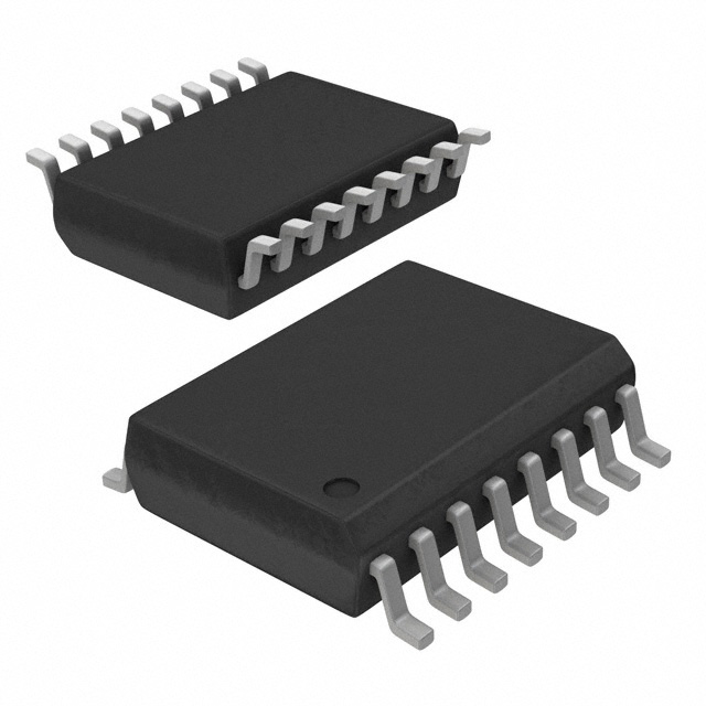
- 16-SOIC (0.295", 7.50mm Width)
- Datasheet:
-
 DS1222S.pdf
- Description:
- IC BANKSWITCH CMOS 16-SOIC
- Quantity:
- Payment:

- Shipping:

Inventory:2,723
Please send an inquiry. Send us your inquiry, and we will respond immediately.
Product details
Overview
DS1222S from Dallas Semiconductor is a 16-bank CMOS memory bank switch IC that selects one of 16 static RAM banks via software-controlled pattern recognition on four address inputs (AW–AZ), operates at 4.5–5.5 V, supports 0°C to 70°C industrial temperature range, and features 15 ns CEO propagation delay. It enables microprocessor address expansion without additional address lines in embedded memory systems.
For engineers reviewing the DS1222S datasheet, DS1222S pinout, DS1222S application, or DS1222S equivalent, key selection considerations include its 16-pin SOIC package, bank-select output timing behavior, power-fail input (PFI) initialization requirement, ±10% VCC tolerance, and pattern-matching bank-switching protocol requiring consecutive 16-bit address sequences.
Technical Context
The DS1222S implements a deterministic 16-bit pattern-matching engine on AW–AZ inputs to decode bank selection, with bit positions 11–15 defining the enabled bank per Table 2. Initialization forces all BS1–BS4 low and CEO high at power-up, contingent on PFI being low prior to power-on.
Bank switching occurs on the rising edge of CEI after full 16-cycle match; CEO follows CEI with ≤15 ns delay, and BS outputs remain latched until next valid pattern. The device requires an initial "1111" read cycle on AW–AZ to synchronize pattern entry and uses no internal clock-timing relies entirely on external CEI strobing.
Key Specifications
| Parameter | Value and Actual Design Meaning |
|---|---|
| VCC Range | 4.5 V to 5.5 V - supports standard +5 V systems with ±10% tolerance, eliminating need for precision regulation |
| Operating Temp | 0°C to 70°C - qualified for commercial/industrial ambient environments without derating |
| Propagation Delay | tPD ≤15 ns - ensures tight timing alignment between CEI and CEO for synchronous memory enable control |
| Input Leakage | ±1.0 µA - minimizes bus loading and preserves signal integrity on shared address lines |
| Output Drive | IOL = +4.0 mA @ 0.4 V - sufficient to directly drive TTL-compatible enable inputs of multiple SRAM devices |
| Pattern Length | 16 consecutive address cycles - mandates precise firmware sequencing; first 11 bits fixed, last 5 define bank via AW–AZ |
Pinout & Package
DS1222S is supplied in a 16-pin SOIC (300-mil) surface-mount package with standard JEDEC MS-012AC footprint and 1.27 mm pitch.
| Pin/Terminal | Circuit Role | Design Meaning |
|---|---|---|
| AW–AZ | Address Input | Four bidirectional address lines used sequentially over 16 cycles to input pattern; AW determines bank number in final 5 bits |
| CEI | Chip Enable Input | Active-low strobe that clocks each address bit into internal shift register; rising edge triggers bank update if pattern matched |
| CEO | Chip Enable Output | Active-high output mirroring CEI with ≤15 ns delay; used to gate memory chip select signals |
| BS1–BS4 | Bank Select Output | Four open-drain or push-pull outputs (per datasheet logic table) encoding selected bank 0–15 as binary-coded 4-bit state |
| PFI | Power Fail Input | Must be held low before power-up to guarantee all banks off and CEO high at reset; enables controlled initialization |
| VCC, GND | Power Supply | +5 V supply and ground pins; decoupling required within 10 mm due to 15 ns switching speed |
| NC | No Connection | Pins 9 and 13 are unconnected; must remain floating or tied to GND per layout guidelines |
Key Features
| Feature | Design Value |
|---|---|
| 16-Bank Selection | Enables up to 16 × 64 KB SRAM banks using only 4 address lines-eliminates need for dedicated bank-select I/O ports |
| Software-Controlled Switching | Eliminates external logic or CPLD for bank management; firmware implements pattern sequence without hardware modification |
| Secure Pattern Recognition | Custom patterns available from Dallas Semiconductor prevent unauthorized bank access by rejecting non-matching sequences |
| Automatic Power-Up Reset | All BS outputs forced low and CEO high at startup-ensures known initial state and prevents spurious memory activation |
| Low-Power CMOS | ICC ≤15 mA typical-reduces thermal load in dense memory subsystems and extends battery life in backup-powered applications |
Applications
| Industrial Data Loggers | Legacy Microcontroller Systems |
|---|---|
Use Scenario: Long-term environmental sensor data storage across multiple SRAM banks with periodic power cycling. IC Role / Device Role / Timing Role: DS1222S acts as bank controller, decoding firmware-generated address patterns to activate correct SRAM bank during write/read bursts. Use Value: Enables 1 MB total SRAM capacity using standard 64 KB chips and existing 16-bit address bus-no PCB redesign needed. | Use Scenario: Extending memory space in 8051- or Z80-based controllers where address lines are fully allocated. IC Role / Device Role / Timing Role: DS1222S serves as address-space expander, translating repeated address reads into bank-select commands synchronized to CEI edges. Use Value: Adds 15 additional banks without modifying CPU address decoding logic-preserves legacy firmware compatibility. |
| Nonvolatile Memory Modules | Embedded Test Equipment |
Use Scenario: Combining DS1222S with DS1212 Nonvolatile Controller to manage 16 banks of NV-SRAM for power-loss-safe data capture. IC Role / Device Role / Timing Role: DS1222S provides bank-select outputs (BS1–BS4) that interface directly with DS1212's bank-enable inputs under pattern-match control. Use Value: Achieves seamless fail-safe memory expansion: pattern-triggered bank switching persists across power cycles when backed by lithium coin cell. | Use Scenario: High-reliability automated test fixtures requiring isolated memory segments for concurrent test sequence storage and result logging. IC Role / Device Role / Timing Role: DS1222S isolates test program memory (Bank 0–7) from results buffer (Bank 8–15) using distinct firmware patterns. Use Value: Prevents test corruption during runtime updates-bank boundaries enforced by hardware-level pattern validation, not software flags. |
Equivalent & Alternatives
The following parts are listed as comparable options for similar memory bank switching applications.
| Alternative Part | Technical Difference | Application Difference | Selection Advice |
|---|---|---|---|
| DS1222N | 14-pin DIP package; identical logic, timing, and pattern protocol; same VCC, temp, and leakage specs | Through-hole assembly only; lacks SOIC thermal and density advantages for modern PCBs | Select DS1222N only for prototyping or legacy through-hole production where reflow compatibility is not required |
| MAX695 | 8-bank capability; different pattern length (8-bit); no PFI input; 5V-only operation; 25 ns tPD | Supports fewer banks and lacks power-fail initialization safeguard; lower timing precision | Choose MAX695 only when 8 banks suffice and firmware cannot accommodate DS1222S's 16-cycle sequence |
Compared with DS1222N and MAX695, the DS1222S uniquely delivers 16-bank support in SOIC with guaranteed power-up reset via PFI-critical for systems requiring deterministic memory state after brownout recovery.
Availability
DS1222S is available at Aetrix Electronics and suitable for industrial data loggers, legacy microcontroller systems, nonvolatile memory modules, and embedded test equipment requiring stable component supply and long-term obsolescence management.
Supply support for DS1222S includes scheduled delivery planning, volume procurement assistance, BOM continuity management, traceable sourcing, and lifecycle availability coordination for OEM customers, industrial embedded developers, connected-device designers, and electronics production programs.
Manufacturer
Dallas Semiconductor (now part of Maxim Integrated, then Analog Devices) specialized in precision timing, nonvolatile memory, and mixed-signal interface ICs for industrial and embedded applications.
The DS1222S belongs to the BankSwitch family designed specifically to solve memory address expansion limitations in resource-constrained microcontrollers-enabling scalable SRAM architectures without adding address pins or external logic.
FAQ
What is the required power-up sequence for reliable initialization of the DS1222S?
The DS1222S requires the Power Fail Input (PFI) pin to be held low before VCC reaches 2.0 V. If PFI is high or floating during power-up, the device may initialize with undefined BS outputs and CEO state. This condition is documented in the Operation section: proper initialization guarantees all BS1–BS4 go low and CEO goes high at power-on. Always tie PFI to GND or use a supervisory circuit that asserts PFI low during ramp-up. The DS1222S must see this condition to ensure deterministic reset behavior.
How does the DS1222S interpret the 16-bit pattern, and why is the "1111" preamble necessary?
DS1222S interprets the 16-bit pattern as two concatenated fields: bits 0–10 (fixed per Table 1) followed by bits 11–15 (bank-defining per Table 2). The "1111" read cycle on AW–AZ before pattern entry synchronizes the internal shift register to bit 0. Without it, the device cannot align incoming bits to the expected position, causing failed matches. Each bit is clocked in on CEI low-to-high transitions, and the full 16-cycle sequence must be uninterrupted. The DS1222S validates the entire sequence before updating BS outputs.
Can the DS1222S be used with microcontrollers lacking dedicated address lines AW–AZ?
Yes-the DS1222S repurposes any four general-purpose I/O pins as AW–AZ, provided firmware can generate the precise 16-cycle read sequence with CEI strobing. No dedicated address bus is required. Many 8-bit MCUs (e.g., PIC16F, ATmega) implement this using GPIO bit-banging. The DS1222S does not require address decoding logic-it only needs controlled voltage levels and timing on those four pins. However, CEI must be driven actively, and PFI must be managed per power-up rules.
What is the function of CEO, and how does it relate to CEI in system design?
CEO is an active-high output that mirrors CEI with ≤15 ns propagation delay and is used to enable downstream memory chips. When CEI goes high after a valid 16-bit pattern, CEO rises synchronously to assert chip select on the selected SRAM bank. Unlike CEI, CEO is not an input-it is a buffered, timed replica optimized for driving memory enable inputs. In system design, CEO connects directly to the /CE pin of target SRAMs, while CEI originates from the MCU. The DS1222S thus converts pattern-matched logic into a clean, low-skew memory enable signal.
Is the DS1222S compatible with 3.3 V systems?
No-the DS1222S is specified only for 4.5 V to 5.5 V operation per Recommended DC Operating Conditions. Its VIH minimum is 2.2 V, but VCC must be ≥4.5 V for guaranteed functionality, including pattern recognition accuracy and output drive strength. Attempting 3.3 V operation violates absolute maximum ratings for VCC and risks unreliable bank switching, increased leakage, or permanent damage. For 3.3 V systems, consider level-shifting or alternative bank-switch controllers rated for 3.3 V, not the DS1222S.
DS1222S Specifications
- Product attributes
- Attribute value
- Manufacturer:
- Analog Devices Inc./Maxim Integrated
- Series:
- -
- Package/Case:
- 16-SOIC (0.295", 7.50mm Width)
- Packaging:
- Tube
- Product Status:
- Obsolete
- Controller Type:
- Static RAM (SRAM)
- Voltage - Supply:
- 4.5V ~ 5.5V
- Operating Temperature:
- 0°C ~ 70°C
- Mounting Type:
- Surface Mount
- Supplier Device Package:
- 16-SOIC
DS1222S FAQ
1.How can I place an order for DS1222S through Aetrix?
Please submit a Request for Quotation (RFQ) for DS1222S on Aetrix. Our sales agent will provide a competitive quotation and guide you through the order confirmation once you accept the terms.
2.Are the price and stock information for DS1222S reliable?
The price and inventory of DS1222S are updated periodically and may fluctuate due to market conditions. Stock and pricing data are typically refreshed every 24 hours. Quotation validity for DS1222S is usually 5 days.
3.What payment methods are accepted for DS1222S?
We accept Wire Transfer, PayPal, Credit Card, Western Union, MoneyGram, and Escrow for DS1222S transactions.
Note: Certain payment methods may incur a processing fee.
4.How is shipping managed for DS1222S?
DS1222S orders can be shipped via leading logistics carriers, including DHL, UPS, FedEx, TNT, or Registered Mail.
Once your DS1222S order is processed, you will receive an email with the shipment details and tracking number.
Note: Tracking information may take up to 24 hours to appear. Express delivery typically takes 3–5 business days.
5.How can I obtain technical support or documentation for DS1222S?
For technical support, including DS1222S datasheets, pinout diagrams, or application guidance, please contact our engineering support team. They can provide detailed documentation and assistance for your DS1222S requirements.
6.How does Aetrix verify that DS1222S is sourced from the original manufacturer or authorized distributors?
All DS1222S products on Aetrix are procured from qualified distributors and authorized channels. Our dedicated quality assurance team conducts strict verification, including traceability checks and, if necessary, third-party testing. This ensures that DS1222S meets industry standards.
7.What is the process for return or replacement of DS1222S?
All DS1222S units undergo pre-shipment inspection (PSI). If there is an issue with DS1222S, returns or replacements are accepted under the following conditions:
1.Quantity discrepancies, incorrect items, or visible external defects (such as breakage or corrosion), acknowledged by Aetrix.
2.The issue is reported within 90 days of delivery.
3.The DS1222S part is unused and in its original packaging.
Return procedure for DS1222S:
1.Submit a request within 90 days.
2.Obtain a Return Material Authorization (RMA) from Aetrix.
DS1222S Tags

-
BQ2201SN-N
Texas Instruments
-
DS1314S+
Analog Devices Inc./Maxim Integrated

-
BQ2205LYPW
Texas Instruments

-
MXD1210CSA+
Analog Devices Inc./Maxim Integrated

-
MXD1210CPA+
Analog Devices Inc./Maxim Integrated

-
4RCD0232KC1ATG
Renesas Electronics Corporation
-
DS1312S-2+
Analog Devices Inc./Maxim Integrated
-
DS1314S-2+T&R
Analog Devices Inc./Maxim Integrated

-
DS1321S+
Analog Devices Inc./Maxim Integrated
-
DS1312S+
Analog Devices Inc./Maxim Integrated
-
MXD1210ESA+
Analog Devices Inc./Maxim Integrated
-
DS1321E+
Analog Devices Inc./Maxim Integrated
Tech Hub

A practical engineering guide to 3.3V and 5V logic compatibility, input thresholds, resistor dividers, translator ICs, MOSFET level shifting, I2C pull-ups, timing limits and power-sequencing risks.

The 74HC595 uses push-pull logic outputs, while the TPIC6B595 uses 50 V open-drain DMOS sinks for higher-power loads. This guide compares timing, current limits, 3.3 V interfacing, load wiring, thermal…

The 74HC595 converts serial data into eight stable parallel outputs. This guide covers pin functions, shift and storage timing, OE and MR behavior, drive-current limits, cascading, voltage compatibilit…

A technical comparison of level-sensitive latches and edge-triggered flip-flops, covering timing windows, setup and hold limits, master–slave operation, time borrowing, race-through, HDL inference and…

A D latch stores one bit while Enable controls when data can pass. This reference covers gate-level operation, truth tables, transparency, setup and hold timing, LE versus OE, common ICs and practical …

An SR latch stores one bit through cross-coupled feedback. This engineering reference covers NOR and NAND implementations, truth tables, forbidden-state recovery, gated operation, switch debouncing, fa…

Latch circuits retain one bit through feedback. This technical reference covers SR and D latches, truth tables, transparency, timing limits, latch-versus-flip-flop behavior, applications and common log…

An engineering guide to LED driver operation, constant-current and constant-voltage outputs, linear and switching topologies, dimming, IC selection, calculations, replacement compatibility, and fault c…

Operational amplifier guide covering op amp basics, feedback, ideal vs real op amps, common configurations, buffer circuits, offset, bias current, gain-bandwidth, slew rate, rail-to-rail limits and sel…

Jumper cables guide covering safe connection order, red and black clamp placement, final ground connection, cable gauge, length, clamp quality, copper vs CCA cables, jump starter comparison and battery…


