
 My Inquiry
 My Account


Texas Instruments DS125RT410SQE/NOPB
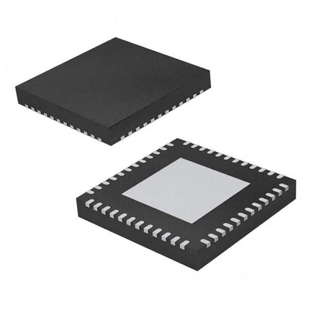
- Part No.:
- DS125RT410SQE/NOPB
- Manufacturer:
- Texas Instruments
- Category:
- Specialized
- Package:
- 48-WFQFN Exposed Pad
- Datasheet:
-
 DS125RT410SQE/NOPB.pdf
- Description:
- IC INTERFACE SPECIALIZED 48WQFN
- Quantity:
- Payment:

- Shipping:

Inventory:2,216
Please send an inquiry. Send us your inquiry, and we will respond immediately.
Product details
Overview
DS125RT410SQE/NOPB from Texas Instruments is a quad-channel, low-power retimer IC for high-speed serial links, featuring adaptive CTLE (up to 34-dB boost at 5 GHz), CDR with ≈300 ps latency, and programmable transmit de-emphasis (–15 dB) and VOD (600–1300 mVp-p). It operates across 9.8–12.5 Gbps and submultiples (÷2/4/8) to support 10GbE, CPRI, and Interlaken in backplane and optical module interfaces.
For engineers reviewing the DS125RT410SQE/NOPB datasheet, DS125RT410SQE/NOPB pinout, DS125RT410SQE/NOPB application, or DS125RT410SQE/NOPB equivalent, key selection criteria include per-channel data-rate independence, 25-MHz reference-accelerated CDR lock time (as low as 12 ms), on-chip eye monitor + PRBS generator for system bring-up, and WQFN-48 (7 mm × 7 mm) thermal performance (RθJB = 6.1 °C/W).
Technical Context
The DS125RT410SQE/NOPB implements four independent retiming channels, each integrating a fully adaptive continuous-time linear equalizer (CTLE), clock and data recovery (CDR) with PLL bandwidth of 5 MHz, and a CML-compatible differential driver with analog de-emphasis. Its CTLE adapts during lock acquisition using a figure-of-merit algorithm and freezes boost level post-lock unless manually re-triggered.
It uses a 25-MHz ±100-ppm crystal reference solely for VCO coarse calibration-not for PLL training-enabling rapid, robust lock without requiring synchronous input clocks. Signal detection, CDR lock status, and interrupt signaling (loss-of-signal, eye opening violation) are provided per channel via dedicated LVCMOS outputs.
Key Specifications
| Parameter | Value and Actual Design Meaning |
|---|---|
| Data Rate Range | 9.8 to 12.5 Gbps per channel, plus submultiples (÷2, ÷4, ÷8) for protocol flexibility including 10.3125 Gbps (10GbE) and CPRI Line Bit Rates 3–7. |
| Latency | ≈300 ps propagation delay-critical for deterministic timing in switch fabric and ASIC interconnects with tight jitter budgets. |
| CTLE Boost | Up to 34-dB gain at 5 GHz-compensates up to ~40-inch FR-4 stripline loss while maintaining BER < 1×10⁻¹⁵. |
| Transmit VOD | 600–1300 mVp-p, software-programmable per channel-enables optimization for varying channel loss and receiver sensitivity. |
| De-emphasis Range | Adjustable to –15 dB-reduces ISI in long copper traces and improves signal integrity at receiver input. |
| Power Dissipation | 150 mW per channel typical (660 mW total)-supports dense integration in space-constrained optical modules and line cards. |
| Supply Voltage | Single 2.5 V ±5%-simplifies power delivery and reduces board-level DC-DC count versus dual-rail alternatives. |
Pinout & Package
DS125RT410SQE/NOPB is housed in a thermally enhanced 48-pin WQFN package (7.00 mm × 7.00 mm, 0.5 mm pitch) with exposed thermal pad (DAP) requiring ≥4 vias to ground plane for optimal thermal performance (RθJB = 6.1 °C/W).
| Pin/Terminal | Circuit Role | Design Meaning |
|---|---|---|
| RXPn / RXNn (n=0–3) | Differential CML input pair | 100 Ω differential input impedance; accepts noisy signals from backplanes or SFP+ DAC cables for equalization and retiming. |
| TXPn / TXNn (n=0–3) | Differential CML output pair | 100 Ω differential output impedance; drives clean, de-emphasized signals to downstream receivers or optical modulators. |
| LPF_CP_n / LPF_REF_n (n=0–3) | CDR loop filter connection | Requires 22 nF ±10% capacitor per channel to set PLL stability and jitter transfer characteristics. |
| LOCK_n / ADDR_n (n=0–3) | Shared CDR lock indicator / SMBus address strap | Indicates per-channel CDR lock status at power-up; doubles as SMBus slave address configuration when strapped. |
| REFCLK_IN / REFCLK_OUT | 25-MHz reference clock I/O | Input enables fast VCO calibration; buffered output supports daisy-chaining multiple DS125RT410 devices on one board. |
| SDA / SDC / EN_SMB | SMBus interface control | 2.5-V/3.3-V tolerant open-drain pins for register configuration or EEPROM-based initialization in master mode. |
Key Features
| Feature | Design Value |
|---|---|
| Per-channel rate independence | Each of four channels locks autonomously to different data rates (9.8–12.5 Gbps) and subrates-enables mixed-protocol systems like 10GbE + CPRI on same device. |
| Adaptive CTLE with freeze-on-lock | CTLE adapts during CDR acquisition then holds boost level until reset-prevents dynamic gain shifts that degrade eye stability during steady-state operation. |
| On-chip eye monitor (EOM) + PRBS generator | Real-time eye opening measurement and pattern generation-eliminates need for external BERT during system bring-up and field tuning. |
| Protocol-select fast lock mode | Uses 25-MHz reference to calibrate VCO before CDR lock-reduces lock time to 12 ms (fixed rate) vs. >70 ms without reference, accelerating production test. |
| Programmable output polarity inversion | Per-channel TX polarity flip via SMBus register-resolves PCB layout mismatches (e.g., swapped differential pairs) without hardware rework. |
Applications
| Front-Port SFP+ Optical Modules | Backplane Reach Extension |
|---|---|
Use Scenario: Retiming 10.3125 Gbps NRZ signals from host ASIC to SFP+ optical transceiver over short (<1 m) PCB traces. IC Role / Device Role / Timing Role: DS125RT410SQE/NOPB acts as a signal integrity bridge-equalizing degraded inputs and regenerating clean, low-jitter outputs compliant with SFF-8431. Use Value: Enables use of cost-effective unshielded PCB routing between ASIC and SFP+ cage while meeting 1×10⁻¹⁵ BER requirement. |
Use Scenario: Extending 12.5 Gbps Interlaken lanes across 40-inch FR-4 backplane with >25 dB loss at Nyquist. IC Role / Device Role / Timing Role: DS125RT410SQE/NOPB serves as a mid-plane retimer-restoring signal amplitude and jitter margin before reaching destination ASIC. Use Value: Achieves reliable link operation where passive trace equalization fails, avoiding costly backplane redesign or higher-layer protocols. |
| CPRI Line Interface (Bit Rates 3–7) | Switch Fabric Interconnect |
Use Scenario: Supporting CPRI Option 7 (10.1376 Gbps) between LTE baseband unit and remote radio head over fiber or DAC cable. IC Role / Device Role / Timing Role: DS125RT410SQE/NOPB functions as a protocol-transparent retimer-preserving deterministic latency and phase alignment critical for RF synchronization. Use Value: Maintains <300 ps latency and sub-UI jitter transfer-meeting CPRI's strict timing accuracy requirements for multi-antenna MIMO systems. |
Use Scenario: Connecting high-speed SerDes lanes between network switch ASICs across mid-plane connectors with crosstalk-induced jitter. IC Role / Device Role / Timing Role: DS125RT410SQE/NOPB operates as a jitter-clearing node-suppressing accumulated intersymbol interference and random jitter before clock domain crossing. Use Value: Resets jitter budget for downstream CDRs, enabling stable 12.5 Gbps operation in electrically noisy switch fabric environments. |
Equivalent & Alternatives
The following parts are listed as comparable options for similar retimer applications.
| Alternative Part | Technical Difference | Application Difference | Selection Advice |
|---|---|---|---|
| DS125DF410 | Replaces CTLE with self-calibrating 5-tap DFE-provides superior crosstalk cancellation but higher power (200+ mW/channel) and no reference-clock acceleration. | Better suited for ultra-high-crosstalk environments (e.g., dense QSFP+ cages); less optimal for low-latency, low-power front-port SFP+. | Select DS125DF410 only when measured crosstalk exceeds CTLE correction capability-otherwise DS125RT410SQE/NOPB delivers lower power and faster lock. |
| DS110RT410 | Narrower rate range (8.5–11.3 Gbps); identical architecture and pinout-but lacks support for 12.5 Gbps CPRI Option 7 and 10.3125 Gbps InfiniBand EDR. | Valid for 10GbE and CPRI Options 3–6, but cannot handle full DS125RT410SQE/NOPB rate spectrum. | Use DS110RT410 only in cost-sensitive designs locked to ≤11.3 Gbps standards-DS125RT410SQE/NOPB provides guaranteed headroom for future upgrades. |
Compared with DS125DF410, DS125RT410SQE/NOPB trades DFE-level crosstalk suppression for lower power and faster lock; compared with DS110RT410, it extends rate coverage to 12.5 Gbps while retaining identical footprint and configuration flow-making it the optimal choice for next-generation optical and wireless infrastructure requiring both performance headroom and thermal efficiency.
Availability
DS125RT410SQE/NOPB is available at Aetrix Electronics and suitable for high-speed optical module assembly, telecom base station backplane design, and switch fabric interconnect applications requiring stable component supply, long-term lifecycle assurance, and traceable sourcing.
Supply support for DS125RT410SQE/NOPB includes scheduled delivery planning, volume procurement assistance, BOM continuity management, traceable sourcing, and lifecycle availability coordination for OEM customers, industrial embedded developers, connected-device designers, and electronics production programs.
Manufacturer
Texas Instruments is a global semiconductor leader specializing in analog, embedded processing, and high-speed interface solutions, with decades of expertise in signal integrity and timing ICs.
The DS125RT410SQE/NOPB belongs to TI's high-speed retimer product line-designed specifically for 10–12.5 Gbps serial link conditioning in optical communications, wireless infrastructure, and data center switching equipment.
FAQ
What data rates does the DS125RT410SQE/NOPB support, and how is rate selection implemented?
The DS125RT410SQE/NOPB supports per-channel locking from 9.8 to 12.5 Gbps and associated submultiples (÷2, ÷4, ÷8). Rate selection is configured via SMBus registers (e.g., Register 0x2F bits 7:4) or inferred automatically using the 25-MHz reference clock for VCO calibration. This enables seamless interoperability with 10GbE, CPRI Options 3–7, and Interlaken without firmware changes-each DS125RT410SQE/NOPB channel operates independently at its assigned rate.
Does the DS125RT410SQE/NOPB require an external reference clock, and what happens if it is omitted?
Yes, the DS125RT410SQE/NOPB requires a 25-MHz ±100-ppm crystal oscillator connected to REFCLK_IN for fast VCO calibration. If omitted, CDR lock time increases significantly (e.g., from 12 ms to >70 ms), and false lock risk rises under periodic input patterns. The reference clock is not used in the PLL feedback path-it only accelerates initial frequency acquisition. REFCLK_OUT provides a buffered copy for multi-device synchronization.
How does the adaptive CTLE in the DS125RT410SQE/NOPB differ from fixed-gain equalizers?
The DS125RT410SQE/NOPB's CTLE adapts during CDR lock acquisition using a figure-of-merit algorithm across 32 predefined boost profiles, then freezes the selected setting until manually reset. Unlike fixed-gain equalizers, this ensures optimal compensation for varying channel loss without over-equalization noise amplification. Post-lock stability prevents eye closure drift-critical for sustained BER < 1×10⁻¹⁵ operation in production systems.
Can the DS125RT410SQE/NOPB be configured without an external microcontroller?
Yes-the DS125RT410SQE/NOPB supports SMBus master mode, where it automatically loads configuration from an external EEPROM on power-up using READ_EN and ALL_DONE signals. This eliminates the need for host processor intervention during boot, making it ideal for headless optical modules and standalone retimer cards. Configuration registers-including VOD, de-emphasis, and rate settings-are retained in EEPROM for repeatable, deterministic startup.
What thermal management considerations apply to the DS125RT410SQE/NOPB in a 4-channel active configuration?
In full 4-channel operation, DS125RT410SQE/NOPB dissipates ~660 mW. Its WQFN-48 package relies on the exposed thermal pad (DAP) connected via ≥4 vias to an internal ground plane for heat dissipation. With RθJB = 6.1 °C/W, a 20°C board temperature rise above ambient requires ~120 cm² of 2-oz copper area. Avoid placing thermal vias under adjacent components, and ensure uninterrupted thermal conduction path from DAP to system heatsink or airflow zone.
DS125RT410SQE/NOPB Specifications
- Product attributes
- Attribute value
- Manufacturer:
- Texas Instruments
- Series:
- -
- Package/Case:
- 48-WFQFN Exposed Pad
- Packaging:
- Tape & Reel (TR)
- Product Status:
- Active
- Applications:
- Ethernet
- Interface:
- I2C
- Voltage - Supply:
- 2.375V ~ 2.625V
- Supplier Device Package:
- 48-WQFN (7x7)
- Grade:
- -
- Qualification:
- -
- Mounting Type:
- Surface Mount
DS125RT410SQE/NOPB FAQ
1.How can I place an order for DS125RT410SQE/NOPB through Aetrix?
Please submit a Request for Quotation (RFQ) for DS125RT410SQE/NOPB on Aetrix. Our sales agent will provide a competitive quotation and guide you through the order confirmation once you accept the terms.
2.Are the price and stock information for DS125RT410SQE/NOPB reliable?
The price and inventory of DS125RT410SQE/NOPB are updated periodically and may fluctuate due to market conditions. Stock and pricing data are typically refreshed every 24 hours. Quotation validity for DS125RT410SQE/NOPB is usually 5 days.
3.What payment methods are accepted for DS125RT410SQE/NOPB?
We accept Wire Transfer, PayPal, Credit Card, Western Union, MoneyGram, and Escrow for DS125RT410SQE/NOPB transactions.
Note: Certain payment methods may incur a processing fee.
4.How is shipping managed for DS125RT410SQE/NOPB?
DS125RT410SQE/NOPB orders can be shipped via leading logistics carriers, including DHL, UPS, FedEx, TNT, or Registered Mail.
Once your DS125RT410SQE/NOPB order is processed, you will receive an email with the shipment details and tracking number.
Note: Tracking information may take up to 24 hours to appear. Express delivery typically takes 3–5 business days.
5.How can I obtain technical support or documentation for DS125RT410SQE/NOPB?
For technical support, including DS125RT410SQE/NOPB datasheets, pinout diagrams, or application guidance, please contact our engineering support team. They can provide detailed documentation and assistance for your DS125RT410SQE/NOPB requirements.
6.How does Aetrix verify that DS125RT410SQE/NOPB is sourced from the original manufacturer or authorized distributors?
All DS125RT410SQE/NOPB products on Aetrix are procured from qualified distributors and authorized channels. Our dedicated quality assurance team conducts strict verification, including traceability checks and, if necessary, third-party testing. This ensures that DS125RT410SQE/NOPB meets industry standards.
7.What is the process for return or replacement of DS125RT410SQE/NOPB?
All DS125RT410SQE/NOPB units undergo pre-shipment inspection (PSI). If there is an issue with DS125RT410SQE/NOPB, returns or replacements are accepted under the following conditions:
1.Quantity discrepancies, incorrect items, or visible external defects (such as breakage or corrosion), acknowledged by Aetrix.
2.The issue is reported within 90 days of delivery.
3.The DS125RT410SQE/NOPB part is unused and in its original packaging.
Return procedure for DS125RT410SQE/NOPB:
1.Submit a request within 90 days.
2.Obtain a Return Material Authorization (RMA) from Aetrix.
DS125RT410SQE/NOPB Tags

-
NVT4857UKAZ
NXP Semiconductors

-
TCA8418RTWR
Texas Instruments

-
PCA9546APWR
Texas Instruments

-
MD0100N8-G
Microchip Technology

-
PCA9548APW,118
NXP Semiconductors

-
PCA9540BDP,118
NXP Semiconductors

-
PCA9548APWR
Texas Instruments

-
PCA9546APW,118
NXP Semiconductors

-
PTN3360DBS,518
NXP Semiconductors

-
PCA9546ABS,118
NXP Semiconductors

-
PCA9518PWR
Texas Instruments

-
PCA9545APW,118
NXP Semiconductors
Tech Hub

A practical engineering guide to 3.3V and 5V logic compatibility, input thresholds, resistor dividers, translator ICs, MOSFET level shifting, I2C pull-ups, timing limits and power-sequencing risks.

The 74HC595 uses push-pull logic outputs, while the TPIC6B595 uses 50 V open-drain DMOS sinks for higher-power loads. This guide compares timing, current limits, 3.3 V interfacing, load wiring, thermal…

The 74HC595 converts serial data into eight stable parallel outputs. This guide covers pin functions, shift and storage timing, OE and MR behavior, drive-current limits, cascading, voltage compatibilit…

A technical comparison of level-sensitive latches and edge-triggered flip-flops, covering timing windows, setup and hold limits, master–slave operation, time borrowing, race-through, HDL inference and…

A D latch stores one bit while Enable controls when data can pass. This reference covers gate-level operation, truth tables, transparency, setup and hold timing, LE versus OE, common ICs and practical …

An SR latch stores one bit through cross-coupled feedback. This engineering reference covers NOR and NAND implementations, truth tables, forbidden-state recovery, gated operation, switch debouncing, fa…

Latch circuits retain one bit through feedback. This technical reference covers SR and D latches, truth tables, transparency, timing limits, latch-versus-flip-flop behavior, applications and common log…

An engineering guide to LED driver operation, constant-current and constant-voltage outputs, linear and switching topologies, dimming, IC selection, calculations, replacement compatibility, and fault c…

Operational amplifier guide covering op amp basics, feedback, ideal vs real op amps, common configurations, buffer circuits, offset, bias current, gain-bandwidth, slew rate, rail-to-rail limits and sel…

Jumper cables guide covering safe connection order, red and black clamp placement, final ground connection, cable gauge, length, clamp quality, copper vs CCA cables, jump starter comparison and battery…


