
 My Inquiry
 My Account


Analog Devices Inc./Maxim Integrated DS1315S-33+
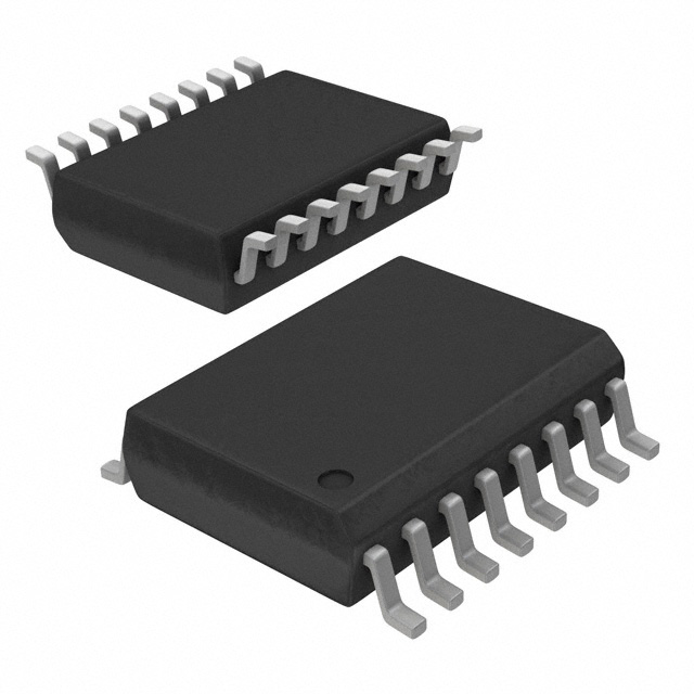
- Part No.:
- DS1315S-33+
- Manufacturer:
- Analog Devices Inc./Maxim Integrated
- Category:
- Real Time Clocks
- Package:
- 16-SOIC (0.295", 7.50mm Width)
- Datasheet:
-
 DS1315S-33+.pdf
- Description:
- IC RTC PHANTOM CHIP PAR 16SOIC
- Quantity:
- Payment:

- Shipping:

Inventory:3,855
Please send an inquiry. Send us your inquiry, and we will respond immediately.
Product details
Overview
DS1315S-33+ from Maxim Integrated is a real-time clock (RTC) and nonvolatile SRAM controller IC combining timekeeping (hundredths of seconds to years, with leap-year correction through 2100) and battery-backed memory control in a single 16-pin SOIC package. It operates at +3.3V, supports dual battery inputs (BAT1/BAT2), and interfaces with external CMOS SRAM or ROM without address-space gaps.
For engineers reviewing the DS1315S-33+ datasheet, DS1315S-33+ pinout, DS1315S-33+ application, or DS1315S-33+ equivalent, key selection criteria include its pattern-based serial access protocol, VCCO switched supply output for SRAM backup, power-fail detection with CEO-driven write protection, and industrial-grade temperature support when ordered as SN variant.
Technical Context
The DS1315S-33+ implements a 64-bit serial pattern recognition protocol (C5h, 3Ah, A3h, 5Ch repeated) to gate access to time registers-prior to match, all CEI/OE/WE activity routes to external memory via CEO; after match, CEO goes high to isolate memory and enable RTC register read/write. Time data is stored in eight BCD-encoded registers accessed sequentially bit-by-bit.
Its nonvolatile controller dynamically selects between RAM mode (ROM/RAM = GND) and ROM mode (ROM/RAM = VCCO): in RAM mode, it supplies VCCO (VCCI − 0.3V max drop) to back up SRAM and performs automatic redundant battery switchover; in ROM mode, CEO asserts low on power fail while retaining internal RTC write protection.
Key Specifications
| Parameter | Value and Actual Design Meaning |
|---|---|
| Supply Voltage | +3.3V ±10% - Enables direct integration into 3.3V logic systems without level-shifting. |
| Operating Temperature | 0°C to +70°C - Commercial-grade thermal range suitable for indoor embedded and instrumentation applications. |
| Timekeeping Accuracy | Leap-year correction valid through year 2100 - Eliminates firmware calendar updates for long-life deployments. |
| VCCO Output | VCCI − 0.3V max drop - Provides stable, low-dropout backup power to external SRAM during main supply failure. |
| Power-Fail Trip Point | 2.8V to 2.97V - Triggers automatic CEO assertion and register write protection before VCC collapses below logic threshold. |
| Crystal Interface | 32.768kHz, 6pF load - Direct connection to standard watch crystal without external capacitors or oscillator circuitry. |
| Pattern Recognition | 64-bit serial sequence (C5h, 3Ah, A3h, 5Ch ×2) - Prevents accidental RTC register access; false-match probability <1 in 10¹⁹. |
Pinout & Package
DS1315S-33+ is housed in a 16-pin Small Outline (SO) package, 300 mils wide, RoHS-compliant (indicated by '+' suffix). Pin 1 is VCC1; pins 9–16 follow standard SOIC numbering with X1/X2 on pins 9/10 and dual ground pins (7 and 16).
| Pin/Terminal | Circuit Role | Design Meaning |
|---|---|---|
| VCC1 | Main power supply input | Accepts +3.3V ±10%; powers internal logic and enables VCCO generation. |
| VCC0 | Switched supply output | Delivers uninterrupted VCCI − 0.3V to external SRAM during power loss. |
| BAT2 | Secondary battery input | Enables redundant battery switchover in RAM mode; highest-voltage battery automatically selected. |
| RST | Hardware reset input | Aborts active data transfer without altering time registers when asserted low (if reset bit = 0). |
| OE | Output enable control | Controls Q output driver during RTC register reads; must be coordinated with CEI/WE for pattern recognition. |
| CEI | Chip enable input | Primary gating signal for all accesses; initiates pattern recognition on first read cycle. |
| CEO | Chip enable output | Drives external memory CE; goes high during RTC access to isolate memory, low on power fail in ROM mode. |
| ROM/RAM | Mode select | GND = RAM mode (VCCO active, battery switchover); VCCO = ROM mode (CEO low on fail, no VCCO drive). |
| X1, X2 | Crystal oscillator terminals | Direct interface to 32.768kHz crystal; internal oscillator circuit eliminates external components. |
| WE | Write enable | Controls data direction during pattern recognition and RTC register writes; used with CEI/OE for timing-critical sequences. |
| BAT1 | Primary battery input | Primary backup source; unused BAT pin must be grounded in single-battery configurations. |
| GND | Ground reference | Two dedicated ground pins (7 and 16) reduce noise coupling and improve power integrity. |
| D | Data input | Serial bit stream input for pattern recognition and RTC register writes; latched on WE/CEI edges. |
| Q | Data output | Serial bit stream output for RTC register reads; driven only when OE and CEI are active post-pattern match. |
Key Features
| Feature | Design Value |
|---|---|
| No address space required | Eliminates need for dedicated memory-mapped I/O or address decoding logic-accesses time registers via serial pattern only. |
| Redundant battery support | Automatic selection of highest-voltage battery (BAT1 or BAT2) ensures continuous SRAM backup in mission-critical systems. |
| Full ±10% VCC operating range | Accommodates typical 3.3V rail tolerances without external regulation or brown-out circuitry. |
| Power-fail detection with CEO control | Internally monitors VCC and forces CEO to VCC or VBAT−0.2V to disable external RAM writes before data corruption occurs. |
| BCD time register format | Simplifies firmware parsing of time/date values; avoids binary-to-BCD conversion overhead in host microcontroller. |
Applications
| Industrial Data Logger | Medical Device Timestamping |
|---|---|
Use Scenario: Standalone battery-powered logger records sensor readings with precise timestamps across multi-year deployments. IC Role / Device Role / Timing Role: DS1315S-33+ serves as primary RTC and SRAM backup controller, maintaining time and volatile log buffer during AC power outages. Use Value: Leap-year correction through 2100 and dual-battery switchover ensure timestamp validity and data retention without firmware intervention. | Use Scenario: Portable diagnostic equipment requires tamper-proof event logging with audit-trail timestamps compliant with FDA 21 CFR Part 11. IC Role / Device Role / Timing Role: DS1315S-33+ provides cryptographically isolated time source and write-protected SRAM storage for critical event logs. Use Value: Pattern-based access and power-fail CEO assertion prevent unauthorized or corrupted time register writes during power transitions. |
| Point-of-Sale Terminal | Network Router Boot Log |
Use Scenario: Retail terminal maintains transaction timestamps and configuration state across frequent power cycles and battery replacements. IC Role / Device Role / Timing Role: DS1315S-33+ synchronizes local time with network NTP on boot while preserving accurate time during offline operation. Use Value: VCCO output sustains SRAM holding last-known time and settings, enabling sub-second time recovery after cold boot. | Use Scenario: Carrier-grade router stores boot diagnostics and crash logs with precise uptime tracking across firmware upgrades and power failures. IC Role / Device Role / Timing Role: DS1315S-33+ acts as persistent time anchor and nonvolatile log buffer controller, decoupled from main SoC power domain. Use Value: Independent power-fail detection and CEO-driven write protection guarantee log integrity even during uncontrolled SoC resets. |
Equivalent & Alternatives
The following parts are listed as comparable options for similar real-time clock and nonvolatile memory controller applications.
| Alternative Part | Technical Difference | Application Difference | Selection Advice |
|---|---|---|---|
| DS1307+ (Maxim) | I²C interface, no pattern recognition; no VCCO output or dual-battery support; only 56-byte RAM. | Lacks integrated SRAM backup control and power-fail write protection; requires external battery management. | Select DS1307+ only for simple I²C RTC needs without nonvolatile memory controller functionality. |
| M41T81SM6TR (STMicroelectronics) | Serial SPI interface, integrated 56-byte RAM, no dual-battery switchover; VBAT directly powers RTC only. | Provides basic RTC+RAM but no switched VCCO output or redundant battery arbitration logic. | Choose M41T81SM6TR when SPI interface and smaller footprint are prioritized over robust SRAM backup control. |
Compared with DS1315S-33+, both alternatives omit the patented 64-bit pattern access protocol, lack VCCO-regulated SRAM backup, and provide no automatic BAT1/BAT2 voltage arbitration-making DS1315S-33+ uniquely suited for high-integrity, long-duration data logging where memory retention and time accuracy must survive multiple power-loss events.
Availability
DS1315S-33+ is available at Aetrix Electronics and suitable for industrial data loggers, medical device timestamping, point-of-sale terminals, network infrastructure diagnostics, and embedded instrumentation requiring stable component supply with long-term lifecycle assurance.
Supply support for DS1315S-33+ includes scheduled delivery planning, volume procurement assistance, BOM continuity management, traceable sourcing, and lifecycle availability coordination for OEM customers, industrial embedded developers, connected-device designers, and electronics production programs.
Manufacturer
Maxim Integrated, now part of Analog Devices, designs precision analog, mixed-signal, and digital ICs for industrial, communications, computing, and consumer applications.
The DS1315S-33+ belongs to Maxim's Phantom Time Chip family, engineered specifically to unify high-accuracy RTC functionality with autonomous nonvolatile SRAM control-enabling zero-software-overhead time stamping and guaranteed data retention in power-constrained systems.
FAQ
What is the primary function of the DS1315S-33+?
The DS1315S-33+ is a combined real-time clock and nonvolatile SRAM controller IC. It maintains accurate time (hundredths of seconds through years with leap-year correction to 2100) while providing battery-backed power switching and write protection for external CMOS SRAM. Its core value lies in eliminating firmware dependency for timekeeping and memory retention during power loss.
How does the DS1315S-33+ interface with external memory?
The DS1315S-33+ uses a serial pattern recognition protocol-not address/data bus-to access its internal time registers. External memory connects directly to CEO, CEI, OE, WE, D, and Q pins. During normal operation, CEO passes through CEI to enable memory; after 64-bit pattern match, CEO goes high to isolate memory and route subsequent cycles to the RTC registers.
Does the DS1315S-33+ support dual battery backup?
Yes, the DS1315S-33+ supports dual battery inputs (BAT1 and BAT2) and automatically selects the higher-voltage source to drive VCCO in RAM mode. This redundancy ensures uninterrupted SRAM backup even if one battery fails, making it ideal for high-reliability applications like industrial loggers and medical devices where data integrity is critical.
What is the purpose of the VCCO pin on the DS1315S-33+?
VCCO is the switched supply output pin that delivers VCCI − 0.3V (max drop) to external SRAM during main power failure. It enables seamless transition from VCC-powered operation to battery-backed SRAM retention without voltage droop or reset. This regulated output is central to the DS1315S-33+'s role as a nonvolatile memory controller-not just an RTC.
Can the DS1315S-33+ operate with a 5V supply?
No, the DS1315S-33+ is rated exclusively for +3.3V ±10% operation. For 5V systems, the pin-compatible DS1315-5+ or DS1315N-5+ variants must be used. The "33" in DS1315S-33+ explicitly denotes 3.3V operation, and applying 5V to DS1315S-33+ exceeds its absolute maximum ratings and will cause permanent damage.
DS1315S-33+ Specifications
- Product attributes
- Attribute value
- Manufacturer:
- Analog Devices Inc./Maxim Integrated
- Series:
- -
- Package/Case:
- 16-SOIC (0.295", 7.50mm Width)
- Packaging:
- Tube
- Product Status:
- Active
- Programmable:
- Not Verified
- Type:
- Phantom Time Chip
- Features:
- Leap Year
- Memory Size:
- -
- Time Format:
- HH:MM:SS:hh (12/24 hr)
- Date Format:
- YY-MM-DD-dd
- Interface:
- Parallel
- Voltage - Supply:
- 3V ~ 3.6V
- Voltage - Supply, Battery:
- 2.5V ~ 3.7V
- Current - Timekeeping (Max):
- 1.1mA @ 3.3V
- Operating Temperature:
- 0°C ~ 70°C
- Mounting Type:
- Surface Mount
- Grade:
- -
- Qualification:
- -
- Supplier Device Package:
- 16-SOIC
DS1315S-33+ FAQ
1.How can I place an order for DS1315S-33+ through Aetrix?
Please submit a Request for Quotation (RFQ) for DS1315S-33+ on Aetrix. Our sales agent will provide a competitive quotation and guide you through the order confirmation once you accept the terms.
2.Are the price and stock information for DS1315S-33+ reliable?
The price and inventory of DS1315S-33+ are updated periodically and may fluctuate due to market conditions. Stock and pricing data are typically refreshed every 24 hours. Quotation validity for DS1315S-33+ is usually 5 days.
3.What payment methods are accepted for DS1315S-33+?
We accept Wire Transfer, PayPal, Credit Card, Western Union, MoneyGram, and Escrow for DS1315S-33+ transactions.
Note: Certain payment methods may incur a processing fee.
4.How is shipping managed for DS1315S-33+?
DS1315S-33+ orders can be shipped via leading logistics carriers, including DHL, UPS, FedEx, TNT, or Registered Mail.
Once your DS1315S-33+ order is processed, you will receive an email with the shipment details and tracking number.
Note: Tracking information may take up to 24 hours to appear. Express delivery typically takes 3–5 business days.
5.How can I obtain technical support or documentation for DS1315S-33+?
For technical support, including DS1315S-33+ datasheets, pinout diagrams, or application guidance, please contact our engineering support team. They can provide detailed documentation and assistance for your DS1315S-33+ requirements.
6.How does Aetrix verify that DS1315S-33+ is sourced from the original manufacturer or authorized distributors?
All DS1315S-33+ products on Aetrix are procured from qualified distributors and authorized channels. Our dedicated quality assurance team conducts strict verification, including traceability checks and, if necessary, third-party testing. This ensures that DS1315S-33+ meets industry standards.
7.What is the process for return or replacement of DS1315S-33+?
All DS1315S-33+ units undergo pre-shipment inspection (PSI). If there is an issue with DS1315S-33+, returns or replacements are accepted under the following conditions:
1.Quantity discrepancies, incorrect items, or visible external defects (such as breakage or corrosion), acknowledged by Aetrix.
2.The issue is reported within 90 days of delivery.
3.The DS1315S-33+ part is unused and in its original packaging.
Return procedure for DS1315S-33+:
1.Submit a request within 90 days.
2.Obtain a Return Material Authorization (RMA) from Aetrix.
DS1315S-33+ Tags

-
MCP7940N-I/SN
Microchip Technology
-
MCP7940MT-I/MNY
Microchip Technology

-
PCF85063ATL/1,118
NXP USA Inc.
-
MCP7940NT-I/SN
Microchip Technology

-
MCP7940NT-I/MS
Microchip Technology
-
MCP7940N-I/MS
Microchip Technology
-
PCF85063AT/AY
NXP USA Inc.

-
PCF85063TP/1Z
NXP Semiconductors

-
PCF85063ATT/AJ
NXP USA Inc.
-
MCP7940NT-E/SN
Microchip Technology
-
MCP7940NT-I/MNY
Microchip Technology
-
MCP79400T-I/SN
Microchip Technology
Tech Hub

A practical engineering guide to 3.3V and 5V logic compatibility, input thresholds, resistor dividers, translator ICs, MOSFET level shifting, I2C pull-ups, timing limits and power-sequencing risks.

The 74HC595 uses push-pull logic outputs, while the TPIC6B595 uses 50 V open-drain DMOS sinks for higher-power loads. This guide compares timing, current limits, 3.3 V interfacing, load wiring, thermal…

The 74HC595 converts serial data into eight stable parallel outputs. This guide covers pin functions, shift and storage timing, OE and MR behavior, drive-current limits, cascading, voltage compatibilit…

A technical comparison of level-sensitive latches and edge-triggered flip-flops, covering timing windows, setup and hold limits, master–slave operation, time borrowing, race-through, HDL inference and…

A D latch stores one bit while Enable controls when data can pass. This reference covers gate-level operation, truth tables, transparency, setup and hold timing, LE versus OE, common ICs and practical …

An SR latch stores one bit through cross-coupled feedback. This engineering reference covers NOR and NAND implementations, truth tables, forbidden-state recovery, gated operation, switch debouncing, fa…

Latch circuits retain one bit through feedback. This technical reference covers SR and D latches, truth tables, transparency, timing limits, latch-versus-flip-flop behavior, applications and common log…

An engineering guide to LED driver operation, constant-current and constant-voltage outputs, linear and switching topologies, dimming, IC selection, calculations, replacement compatibility, and fault c…

Operational amplifier guide covering op amp basics, feedback, ideal vs real op amps, common configurations, buffer circuits, offset, bias current, gain-bandwidth, slew rate, rail-to-rail limits and sel…

Jumper cables guide covering safe connection order, red and black clamp placement, final ground connection, cable gauge, length, clamp quality, copper vs CCA cables, jump starter comparison and battery…


