
 My Inquiry
 My Account


Analog Devices Inc./Maxim Integrated DS1340C-18#
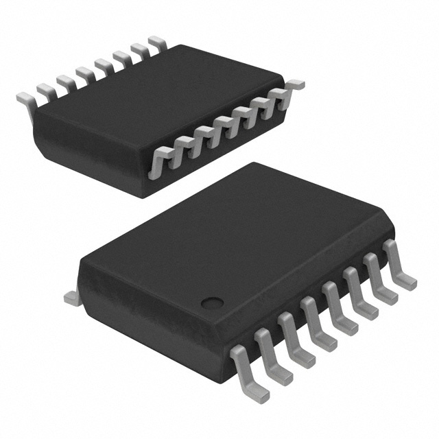
- Part No.:
- DS1340C-18#
- Manufacturer:
- Analog Devices Inc./Maxim Integrated
- Category:
- Real Time Clocks
- Package:
- 16-SOIC (0.295", 7.50mm Width)
- Datasheet:
-
 DS1340C-18#.pdf
- Description:
- IC RTC CLK/CALENDAR I2C 16SOIC
- Quantity:
- Payment:

- Shipping:

Inventory:829
Please send an inquiry. Send us your inquiry, and we will respond immediately.
Product details
Overview
DS1340C-18# from Maxim Integrated is a surface-mount I²C real-time clock/calendar with integrated 32.768kHz crystal, trickle-charge capability on VBACKUP, oscillator stop flag (OSF), and low timekeeping voltage down to 1.3V. It operates across -40°C to +85°C, supports 1.8V supply, and delivers BCD-formatted time/date (seconds to year) with automatic leap-year correction-used in portable medical instruments requiring battery-backed timekeeping with minimal PCB footprint.
For engineers reviewing the DS1340C-18# datasheet, DS1340C-18# pinout, DS1340C-18# application, or DS1340C-18# equivalent, key selection criteria include its 16-pin SO package with integrated crystal, 400kHz I²C interface, VBACKUP trickle-charge resistor configuration (250Ω/2kΩ/4kΩ), OSF flag for oscillator health monitoring, and software calibration via CAL[4:0] bits with ±4.068ppm/−2.034ppm per step.
Technical Context
The DS1340C-18# implements a precision temperature-compensated power-fail detection circuit that switches between VCC and VBACKUP when VCC drops below VPF (1.51–1.71V), maintaining register integrity without halting timekeeping. Its internal oscillator drives a divider chain synchronized to secondary buffers during I²C reads, eliminating read-race conditions.
Trickle charging is enabled only by the exact TCS[3:0] = 1010 pattern in register 08h, selecting diode/resistor combinations (e.g., one diode + 2kΩ) to limit charge current; the OSF bit is edge-triggered and latched until explicitly cleared, providing deterministic oscillator fault detection independent of VCC/VBACKUP voltage levels.
Key Specifications
| Parameter | Value and Actual Design Meaning |
|---|---|
| Supply Voltage | 1.71V to 5.5V - supports 1.8V systems while remaining compatible with legacy 3V/3.3V buses |
| Backup Voltage Range | 1.3V to 3.7V - enables operation from lithium coin cells or supercaps without external regulation |
| I²C Speed | Up to 400kHz Fast Mode - reduces transaction time vs. standard 100kHz, critical for low-power wake-up sequences |
| Timekeeping Accuracy | ±15ppm at +25°C (typical) - derived from factory-trimmed integrated crystal; no external load capacitors required |
| Power-Fail Threshold | 1.51V to 1.71V - precise switchover point ensures reliable backup activation before VCC brownout affects logic |
| Oscillator Stop Flag Delay | 100ms - guarantees OSF assertion after sustained oscillator halt, enabling robust time validity checks |
| Standby Current | 60–100μA at 1.89V - minimizes primary supply drain during host MCU sleep cycles |
Pinout & Package
DS1340C-18# uses a 16-pin small-outline (SO) package with integrated crystal; pins 4–13 are No Connect (N.C.) and must be grounded per datasheet requirement. The package includes internal bias network and crystal mounting structure, eliminating external CL tuning components.
| Pin/Terminal | Circuit Role | Design Meaning |
|---|---|---|
| 1, 2 | X1, X2 | Crystal input/output nodes - internally terminated for 12.5pF load; X1 accepts external 32.768kHz oscillator if needed |
| 3 | VBACKUP | Backup power rail - supports trickle charging via programmable resistor/diode path; UL-recognized for lithium battery safety |
| 4 | GND | Analog/digital ground reference - shared return for VCC, VBACKUP, and I²C lines |
| 5 | SDA | Open-drain I²C data line - requires external pullup; tolerates up to 5.5V pullup voltage regardless of VCC level |
| 6 | SCL | Open-drain I²C clock input - synchronizes all serial transfers; supports standard/fast mode timing |
| 7 | FT/OUT | Configurable output - toggles at 512Hz (FT=1) or reflects OUT bit (FT=0); open-drain, pullup-voltage-flexible |
| 8 | VCC | Main supply input - powers digital core and I²C interface; device fully accessible only above VPF threshold |
| 14–16 | N.C. | No Connection - pins 14 (VBACKUP), 15 (GND), 16 (SDA) are duplicates of pins 3, 4, 5 per 16-pin SO layout; must be grounded |
Key Features
| Feature | Design Value |
|---|---|
| Integrated Crystal | Eliminates 2 external load capacitors and crystal layout sensitivity, reducing BOM count and board area by ~25mm² |
| Software Clock Calibration | Adjusts timekeeping rate in ±2.034ppm to ±4.068ppm steps via CAL[4:0] bits, compensating for crystal aging and temperature drift |
| Oscillator Stop Flag (OSF) | Latched diagnostic bit indicating oscillator failure due to power loss, crystal fault, or EOSC disable-enables firmware validation of time validity |
| Trickle-Charge Programmability | Selects between 250Ω/2kΩ/4kΩ current-limiting resistors and diode/no-diode paths via register 08h, supporting diverse backup sources (coin cell, supercap, rechargeable) |
| Automatic Power-Switch Logic | Seamlessly transitions between VCC and VBACKUP without glitch or register corruption when VCC crosses VPF, preserving RTC state across power cycles |
Applications
| Portable Medical Monitors | Point-of-Sale Terminals |
|---|---|
Use Scenario: Battery-powered ECG or glucose meter logging timestamps during intermittent sensor sampling and wireless upload. IC Role / Device Role / Timing Role: Primary timekeeping source maintaining accurate wall-clock time during 72-hour battery operation with zero VCC supply. Use Value: Integrated crystal and 1.3V timekeeping enable >10-year coin-cell backup life; OSF flag validates timestamp integrity before clinical data transmission. | Use Scenario: Compact retail terminal with offline transaction logging during brief network outages. IC Role / Device Role / Timing Role: Synchronized event timer generating audit trails for sales receipts and inventory updates. Use Value: 400kHz I²C interface accelerates time-register reads during high-throughput checkout; VBACKUP trickle charging extends supercap lifetime beyond 5 years. |
| Industrial Data Loggers | Telecom Network Edge Devices |
Use Scenario: Ruggedized environmental sensor node recording temperature/humidity every 15 minutes across −40°C to +85°C ambient range. IC Role / Device Role / Timing Role: Temperature-stable RTC providing UTC-aligned timestamps for distributed sensor fusion. Use Value: Factory-calibrated ±15ppm accuracy eliminates field recalibration; N.C. pins grounded to suppress noise coupling into crystal circuitry. | Use Scenario: Small-cell base station maintaining synchronization during GPS signal loss or holdover periods. IC Role / Device Role / Timing Role: Backup timekeeper ensuring packet timestamp continuity during PTP master failover. Use Value: Power-fail detect circuit activates VBACKUP within 2ms (tREC), preventing time discontinuity in IEEE 1588-compliant timing stacks. |
Equivalent & Alternatives
The following parts are listed as comparable options for similar RTC applications.
| Alternative Part | Technical Difference | Application Difference | Selection Advice |
|---|---|---|---|
| STMicroelectronics M41T00M6F | Pin-compatible but lacks integrated crystal and trickle-charge circuitry; requires external 32.768kHz crystal and discrete charging components | Higher BOM cost and larger PCB footprint; no OSF flag or software calibration | Choose when legacy ST design reuse is prioritized over space/power savings |
| Maxim Integrated DS3231SN | Features TCXO (±2ppm) and higher-accuracy temperature compensation; no VBACKUP trickle-charge support | Better long-term stability but incompatible with battery-charging architectures; 16-pin SO package same footprint | Prefer for precision timing-critical systems where backup charging is handled externally |
Compared with DS1340C-18#, the M41T00M6F requires additional passive components and offers no timekeeping calibration, while the DS3231SN delivers superior accuracy but removes the ability to recharge backup sources-making DS1340C-18# optimal for space-constrained, battery-charged embedded systems needing moderate accuracy and integrated crystal simplicity.
Availability
DS1340C-18# is available at Aetrix Electronics and suitable for portable medical monitors, point-of-sale terminals, and industrial data loggers requiring stable component supply across extended temperature ranges and long production lifecycles.
Supply support for DS1340C-18# includes scheduled delivery planning, volume procurement assistance, BOM continuity management, traceable sourcing, and lifecycle availability coordination for OEM customers, industrial embedded developers, connected-device designers, and electronics production programs.
Manufacturer
Maxim Integrated (now part of Analog Devices) designs precision analog and mixed-signal ICs for power, sensing, and timing applications, with emphasis on low-power, high-reliability solutions for industrial and medical markets.
The DS1340 product line delivers highly integrated RTCs with backup power management, targeting applications where board space, battery life, and time validity assurance are critical-such as handheld diagnostics and edge telemetry devices.
FAQ
What is the function of the OSF bit in DS1340C-18#?
The OSF (Oscillator Stop Flag) bit in DS1340C-18# is a latched status indicator located in register 09h, bit 7. It asserts logic 1 when the internal 32.768kHz oscillator halts due to power loss, crystal fault, EOSC disable, or noise interference. DS1340C-18# retains this flag until firmware explicitly writes 0 to it, enabling reliable validation of time/date validity before use in safety-critical logs or audits.
How does DS1340C-18# handle power switching between VCC and VBACKUP?
DS1340C-18# uses an internal comparator with a 1.51V–1.71V VPF threshold to monitor VCC. When VCC falls below VPF, DS1340C-18# automatically switches power to VBACKUP while blocking register access-but continues timekeeping uninterrupted. Upon VCC recovery above VPF, DS1340C-18# waits 2ms (tREC) before re-enabling I²C access, ensuring stable register state restoration.
Can DS1340C-18# operate with a 3.3V supply?
Yes, DS1340C-18# supports 3.3V operation: its VCC range spans 1.71V to 5.5V, and the "-18" suffix denotes 1.8V nominal compatibility-not exclusivity. At 3.3V, DS1340C-18# draws 108–200μA active current and maintains full I²C functionality, including 400kHz Fast Mode, while retaining all features like trickle charging and OSF flag reporting.
What is the purpose of the TCS bits in DS1340C-18# register 08h?
The TCS[3:0] bits (bits 7–4) in DS1340C-18# register 08h control trickle-charge activation and configuration. Only the binary pattern 1010 enables charging; all other values disable it. When enabled, DS1340C-18# uses these bits alongside DS[1:0] and ROUT[1:0] to select diode presence and current-limiting resistor value (250Ω/2kΩ/4kΩ), allowing safe, programmable charging of VBACKUP sources like supercaps.
Does DS1340C-18# require external load capacitors for its integrated crystal?
No, DS1340C-18# does not require external load capacitors. Its integrated 32.768kHz crystal is factory-matched to the internal oscillator's 12.5pF capacitive load, eliminating CL tuning components. This integration reduces PCB area, simplifies layout, and improves EMI immunity-confirmed in the DS1340C-specific section of the datasheet, which states "no external resistors or capacitors to operate."
DS1340C-18# Specifications
- Product attributes
- Attribute value
- Manufacturer:
- Analog Devices Inc./Maxim Integrated
- Series:
- -
- Package/Case:
- 16-SOIC (0.295", 7.50mm Width)
- Packaging:
- Tube
- Product Status:
- Active
- Programmable:
- Not Verified
- Type:
- Clock/Calendar
- Features:
- Leap Year, Trickle-Charger
- Memory Size:
- -
- Time Format:
- HH:MM:SS (24 hr)
- Date Format:
- YY-MM-DD-dd
- Interface:
- I2C, 2-Wire Serial
- Voltage - Supply:
- 1.71V ~ 5.5V
- Voltage - Supply, Battery:
- 1.3V ~ 3.7V
- Current - Timekeeping (Max):
- 100µA @ 1.89V
- Operating Temperature:
- -40°C ~ 85°C
- Mounting Type:
- Surface Mount
- Grade:
- -
- Qualification:
- -
- Supplier Device Package:
- 16-SOIC
DS1340C-18# FAQ
1.How can I place an order for DS1340C-18# through Aetrix?
Please submit a Request for Quotation (RFQ) for DS1340C-18# on Aetrix. Our sales agent will provide a competitive quotation and guide you through the order confirmation once you accept the terms.
2.Are the price and stock information for DS1340C-18# reliable?
The price and inventory of DS1340C-18# are updated periodically and may fluctuate due to market conditions. Stock and pricing data are typically refreshed every 24 hours. Quotation validity for DS1340C-18# is usually 5 days.
3.What payment methods are accepted for DS1340C-18#?
We accept Wire Transfer, PayPal, Credit Card, Western Union, MoneyGram, and Escrow for DS1340C-18# transactions.
Note: Certain payment methods may incur a processing fee.
4.How is shipping managed for DS1340C-18#?
DS1340C-18# orders can be shipped via leading logistics carriers, including DHL, UPS, FedEx, TNT, or Registered Mail.
Once your DS1340C-18# order is processed, you will receive an email with the shipment details and tracking number.
Note: Tracking information may take up to 24 hours to appear. Express delivery typically takes 3–5 business days.
5.How can I obtain technical support or documentation for DS1340C-18#?
For technical support, including DS1340C-18# datasheets, pinout diagrams, or application guidance, please contact our engineering support team. They can provide detailed documentation and assistance for your DS1340C-18# requirements.
6.How does Aetrix verify that DS1340C-18# is sourced from the original manufacturer or authorized distributors?
All DS1340C-18# products on Aetrix are procured from qualified distributors and authorized channels. Our dedicated quality assurance team conducts strict verification, including traceability checks and, if necessary, third-party testing. This ensures that DS1340C-18# meets industry standards.
7.What is the process for return or replacement of DS1340C-18#?
All DS1340C-18# units undergo pre-shipment inspection (PSI). If there is an issue with DS1340C-18#, returns or replacements are accepted under the following conditions:
1.Quantity discrepancies, incorrect items, or visible external defects (such as breakage or corrosion), acknowledged by Aetrix.
2.The issue is reported within 90 days of delivery.
3.The DS1340C-18# part is unused and in its original packaging.
Return procedure for DS1340C-18#:
1.Submit a request within 90 days.
2.Obtain a Return Material Authorization (RMA) from Aetrix.
DS1340C-18# Tags

-
MCP7940N-I/SN
Microchip Technology
-
MCP7940MT-I/MNY
Microchip Technology

-
PCF85063ATL/1,118
NXP USA Inc.
-
MCP7940NT-I/SN
Microchip Technology

-
MCP7940NT-I/MS
Microchip Technology
-
MCP7940N-I/MS
Microchip Technology
-
PCF85063AT/AY
NXP USA Inc.

-
PCF85063TP/1Z
NXP Semiconductors

-
PCF85063ATT/AJ
NXP USA Inc.
-
MCP7940NT-E/SN
Microchip Technology
-
MCP7940NT-I/MNY
Microchip Technology
-
MCP79400T-I/SN
Microchip Technology
Tech Hub

A practical engineering guide to 3.3V and 5V logic compatibility, input thresholds, resistor dividers, translator ICs, MOSFET level shifting, I2C pull-ups, timing limits and power-sequencing risks.

The 74HC595 uses push-pull logic outputs, while the TPIC6B595 uses 50 V open-drain DMOS sinks for higher-power loads. This guide compares timing, current limits, 3.3 V interfacing, load wiring, thermal…

The 74HC595 converts serial data into eight stable parallel outputs. This guide covers pin functions, shift and storage timing, OE and MR behavior, drive-current limits, cascading, voltage compatibilit…

A technical comparison of level-sensitive latches and edge-triggered flip-flops, covering timing windows, setup and hold limits, master–slave operation, time borrowing, race-through, HDL inference and…

A D latch stores one bit while Enable controls when data can pass. This reference covers gate-level operation, truth tables, transparency, setup and hold timing, LE versus OE, common ICs and practical …

An SR latch stores one bit through cross-coupled feedback. This engineering reference covers NOR and NAND implementations, truth tables, forbidden-state recovery, gated operation, switch debouncing, fa…

Latch circuits retain one bit through feedback. This technical reference covers SR and D latches, truth tables, transparency, timing limits, latch-versus-flip-flop behavior, applications and common log…

An engineering guide to LED driver operation, constant-current and constant-voltage outputs, linear and switching topologies, dimming, IC selection, calculations, replacement compatibility, and fault c…

Operational amplifier guide covering op amp basics, feedback, ideal vs real op amps, common configurations, buffer circuits, offset, bias current, gain-bandwidth, slew rate, rail-to-rail limits and sel…

Jumper cables guide covering safe connection order, red and black clamp placement, final ground connection, cable gauge, length, clamp quality, copper vs CCA cables, jump starter comparison and battery…


