
 My Inquiry
 My Account


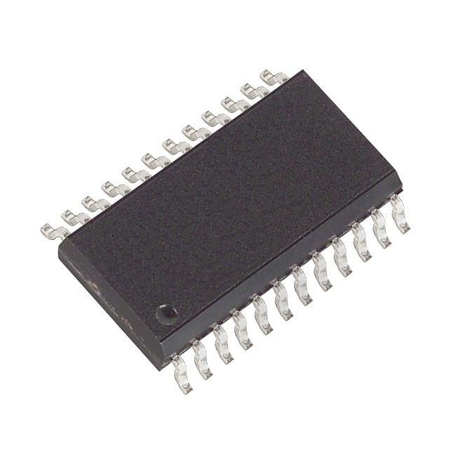
Analog Devices Inc./Maxim Integrated DS17285S-3/T&R
- Part No.:
- DS17285S-3/T&R
- Manufacturer:
- Analog Devices Inc./Maxim Integrated
- Category:
- Real Time Clocks
- Package:
- 24-SOIC (0.295", 7.50mm Width)
- Datasheet:
-
 DS17285S-3/T&R.pdf
- Description:
- IC RTC CLK/CALENDAR PAR 24SOIC
- Quantity:
- Payment:

- Shipping:

Inventory:1,730
Please send an inquiry. Send us your inquiry, and we will respond immediately.
Product details
Overview
DS17285S-3/T&R from Maxim Integrated is a 24-pin real-time clock/calendar IC with integrated power-control circuitry, 114 bytes of battery-backed NV SRAM, 2kB extended NV SRAM, and multiplexed byte-wide interface. It supports +3.0V operation, automatic VCC-to-VBAT/VBAUX switchover on power fail, and system wake-up via time-of-day alarm or external kickstart (KS) input. Used in utility meters and industrial embedded systems requiring long-term timekeeping under intermittent power.
For engineers reviewing the DS17285S-3/T&R datasheet, DS17285S-3/T&R pinout, DS17285S-3/T&R application, or DS17285S-3/T&R equivalent, key selection considerations include its 3V-only supply range, EDIP-compatible 24-pin DIP package with no X1/X2 pins, PWR output for system power-on control, IRQ interrupt with six maskable flags, and support for BCD/binary time format with leap-year compensation through 2099.
Technical Context
The DS17285S-3/T&R implements a temperature-compensated voltage monitor to detect VCC drop below 2.5V–2.7V (VPF), triggering automatic switchover to VBAT or VBAUX. Its internal oscillator is disabled in this part variant-X1 and X2 pins are NC-as confirmed by EDIP package documentation and pin description tables.
It uses a multiplexed AD0–AD7 bus with ALE-latched addressing, supporting read/write cycles at ≥360ns cycle time under 3V operation. Control registers A–D and extended bank-1 registers (e.g., 48h/49h for century/date alarm) enable configuration of alarm masking, square-wave output (SQW), and power-control logic including PWR assertion and KS-triggered wake-up.
Key Specifications
| Parameter | Value and Actual Design Meaning |
|---|---|
| Supply Voltage | +2.7V to +3.7V - Supports single 3V system rail; invalid above 3.7V or below 2.7V |
| Power-Fail Threshold | 2.5V–2.7V (VPF) - Triggers automatic backup power switchover and inhibits access until recovery |
| Standby Current | 0.5–2.0mA (ICCS) - Measured with CS=RD=WR=VCC, defines minimum system sleep power draw |
| VBAT/VBAUX Current | 50–400nA (oscillator off), 500–700nA (oscillator on) - Enables >10-year data retention on coin cell |
| Memory Capacity | 114 bytes user NV SRAM + 2048 bytes extended NV SRAM - Retained during VCC loss; RCLR pin clears only base RAM |
| Time Accuracy | Factory-trimmed ±1 minute/month at 25°C - Applies to DS17287 EDIP variant; DS17285S-3/T&R requires external crystal |
| Interface Timing | tCYC ≥360ns, tDHR ≤90ns - Defines minimum microcontroller bus speed for reliable register access |
Pinout & Package
DS17285S-3/T&R is supplied in a 24-pin plastic DIP (PDIP) package, RoHS-compliant and tape-and-reel packaged (T&R). Pin layout matches standard DS12887 footprint for drop-in replacement in legacy designs. X1 and X2 pins are not connected (N.C.) - oscillator must be provided externally or omitted per application.
| Pin/Terminal | Circuit Role | Design Meaning |
|---|---|---|
| AD0–AD7 | Multiplexed address/data bus | Latches address on ALE falling edge; carries data during RD/WR cycles - requires external latch (e.g., 74LS373) |
| CS | Active-low chip select | Must be low throughout RD/WR; enables device decoding - tied low for simple systems |
| ALE | Address latch enable | Falling edge captures address into internal latch - critical timing signal for bus demultiplexing |
| RD / WR | Active-low read/write strobes | Control data direction and timing - WR latches write data, RD enables output drivers |
| IRQ | Open-drain interrupt request | Asserts low on alarm/maskable event - requires external pullup; shares interrupt bus with other open-drain devices |
| PWR | Open-drain power-on control | Drives external power supply enable - activated by KS or wake-up alarm; software-controllable after boot |
| KS | Active-low kickstart input | Triggers PWR when VCC absent - requires VBAUX present and ABE bit set; pulled up to VBAUX |
| RCLR | Active-low RAM clear | Resets 114-byte base RAM to 0xFF - intended for manual reset via switch; internally pulled up |
| VCC | +3V primary supply | Enables full register access above VPF; below VPF, device enters low-power mode and disables bus |
| VBAT / VBAUX | Backup power inputs | VBAT powers RTC core; VBAUX required for KS/wake-up - both accept 2.5–3.7V lithium cells |
Key Features
| Feature | Design Value |
|---|---|
| Leap-year compensated calendar | Automatically adjusts end-of-month dates through year 2099 - eliminates firmware date logic in metering and logging applications |
| System power-on control | PWR output enables external DC-DC converter or LDO - allows complete system sleep between utility meter reads or security events |
| 64-bit silicon serial number | Factory-programmed unique ID - enables secure device authentication and field-level asset tracking in networked infrastructure |
| Six maskable interrupts | Independent PIE/AIE/UIE/SQWE/AF/UF flags feed single IRQ pin - reduces MCU GPIO count while supporting alarm, update, and power-fail event handling |
| Software-configurable time format | 12/24-hour mode with AM/PM indicator controlled by register bit - simplifies UI integration across global markets without hardware change |
| Crystal select bit | Configures internal load capacitance for 6pF or 12.5pF crystals - ensures optimal oscillation margin across production lots and temperature ranges |
Applications
| Smart Utility Metering | Industrial Data Logger |
|---|---|
Use Scenario: Electricity/gas/water meter records consumption timestamps and stores tamper events during grid outages. IC Role / Device Role / Timing Role: Primary timekeeping and nonvolatile event logging engine with autonomous wake-up on billing interval. Use Value: Maintains accurate time and retains 2kB usage history for >10 years on coin cell - meets ANSI C12.1 and IEC 62056 compliance requirements. |
Use Scenario: Remote environmental sensor node samples temperature/humidity every 15 minutes and logs to local flash. IC Role / Device Role / Timing Role: Low-power timebase and timestamp generator synchronized to UTC via periodic GPS sync. Use Value: Enables deterministic wake-up scheduling and precise time-stamping without MCU involvement - extends battery life by 40% vs. RTC-less designs. |
| Access Control Panel | Network Infrastructure Clock |
Use Scenario: Door controller logs entry attempts and triggers alarms based on time-of-day schedules. IC Role / Device Role / Timing Role: Real-time scheduler and audit trail timestamp source with battery-backed memory for offline operation. Use Value: Guarantees time continuity during AC power loss; stores 114-byte access log and 2kB extended event buffer - satisfies UL 294 audit trail requirements. |
Use Scenario: Managed Ethernet switch maintains system uptime counter and synchronizes SNMP trap timestamps. IC Role / Device Role / Timing Role: Standalone time reference for system health monitoring and diagnostics when NTP unavailable. Use Value: Provides monotonic, drift-compensated timebase independent of network stack - ensures accurate fault correlation across distributed switches. |
Equivalent & Alternatives
The following parts are listed as comparable options for similar real-time clock applications.
| Alternative Part | Technical Difference | Application Difference | Selection Advice |
|---|---|---|---|
| DS1307+T&R | I²C interface, no PWR/KS pins, 56 bytes NV RAM, no extended RAM or power-control logic | Lower-cost consumer-grade timing; unsuitable for system power management or industrial wake-up | Select DS1307 only for space-constrained, low-pin-count designs where system-level power control is handled externally |
| PCF8583P+T&R | 400kHz I²C, 256 bytes NV RAM, no alarm masking or PWR output, operates at 2.5–6.0V | Legacy automotive infotainment timing; lacks kickstart, century register, and UL recognition | Choose PCF8583P for cost-sensitive automotive modules requiring basic calendar but no industrial power sequencing |
Compared with DS17285S-3/T&R, DS1307 offers simpler integration but no system power control or extended memory, while PCF8583P provides more RAM but lacks UL recognition, wake-up capability, and leap-year accuracy through 2099 - making DS17285S-3/T&R the only option meeting utility meter certification and industrial power-gating requirements.
Availability
DS17285S-3/T&R is available at Aetrix Electronics and suitable for smart utility metering, industrial data loggers, access control panels, and network infrastructure equipment requiring stable component supply across multi-year production cycles.
Supply support for DS17285S-3/T&R includes scheduled delivery planning, volume procurement assistance, BOM continuity management, traceable sourcing, and lifecycle availability coordination for OEM customers, industrial embedded developers, connected-device designers, and electronics production programs.
Manufacturer
Maxim Integrated (now part of Analog Devices) designs precision analog, mixed-signal, and power management ICs for industrial, medical, and communications applications.
The DS17285S-3/T&R belongs to Maxim's legacy real-time clock family engineered for high-reliability embedded systems requiring battery-backed timekeeping, system-level power sequencing, and regulatory compliance (UL recognition).
FAQ
What is the operating voltage range for DS17285S-3/T&R?
The DS17285S-3/T&R operates from +2.7V to +3.7V on VCC. Operation outside this range risks functional failure or damage. VBAT and VBAUX inputs accept 2.5V–3.7V for backup power. The device includes a precision voltage monitor that triggers automatic switchover to backup power when VCC drops below 2.5V–2.7V (VPF), ensuring continuous RTC operation and data retention in DS17285S-3/T&R.
Does DS17285S-3/T&R include an integrated crystal or battery?
No, DS17285S-3/T&R is the PDIP version without integrated crystal or battery - it requires an external 32.768kHz crystal connected to X1/X2 pins. In contrast, the DS17287 variant packages crystal and lithium cell in an EDIP module. DS17285S-3/T&R's X1 and X2 pins are functional and must be used; they are not NC. This distinction is critical for board layout and BOM accuracy in DS17285S-3/T&R designs.
How does the PWR output function in DS17285S-3/T&R?
The PWR pin in DS17285S-3/T&R is an open-drain output that drives external power supplies. It activates automatically on wake-up alarm or KS pin transition when VCC is absent, and remains software-controllable via register bits after system boot. A pullup resistor to VBAUX (≤3.9V) is required. This enables DS17285S-3/T&R to serve as the central power sequencer in battery-operated infrastructure nodes - a capability absent in most competing RTCs.
Can DS17285S-3/T&R operate in both 12-hour and 24-hour time formats?
Yes, DS17285S-3/T&R supports both formats via the 24/12 bit in Register B. In 12-hour mode, the MSB of the hours byte indicates PM. The device retains all time/calendar data in double-buffered registers, enabling glitch-free reads during updates. Format selection is persistent across power cycles and requires reinitialization only if changed - a feature confirmed in DS17285S-3/T&R's control register specification and essential for global UI localization.
What is the data retention period for DS17285S-3/T&R's NV SRAM?
DS17285S-3/T&R guarantees ≥10 years of data retention in its 114-byte base NV SRAM and 2048-byte extended NV SRAM when backed by a 3.0V lithium coin cell at +25°C, per Maxim's characterization data. Retention depends on VBAT/VBAUX voltage stability and temperature; operation below 2.5V or above +85°C degrades endurance. This 10-year spec is validated for DS17285S-3/T&R under standard conditions and forms the basis for utility meter certification lifetimes.
DS17285S-3/T&R Specifications
- Product attributes
- Attribute value
- Manufacturer:
- Analog Devices Inc./Maxim Integrated
- Series:
- -
- Package/Case:
- 24-SOIC (0.295", 7.50mm Width)
- Packaging:
- Tape & Reel (TR)
- Product Status:
- Obsolete
- Programmable:
- Not Verified
- Type:
- Clock/Calendar
- Features:
- Alarm, Daylight Savings, Leap Year, NVSRAM, Square Wave Output
- Memory Size:
- 2KB
- Time Format:
- HH:MM:SS (12/24 hr)
- Date Format:
- YY-MM-DD-dd
- Interface:
- Parallel
- Voltage - Supply:
- 2.7V ~ 3.7V
- Voltage - Supply, Battery:
- 2.5V ~ 3.7V
- Current - Timekeeping (Max):
- 2mA @ 2.7V ~ 3.7V
- Operating Temperature:
- 0°C ~ 70°C
- Mounting Type:
- Surface Mount
- Grade:
- -
- Qualification:
- -
- Supplier Device Package:
- 24-SOIC
DS17285S-3/T&R FAQ
1.How can I place an order for DS17285S-3/T&R through Aetrix?
Please submit a Request for Quotation (RFQ) for DS17285S-3/T&R on Aetrix. Our sales agent will provide a competitive quotation and guide you through the order confirmation once you accept the terms.
2.Are the price and stock information for DS17285S-3/T&R reliable?
The price and inventory of DS17285S-3/T&R are updated periodically and may fluctuate due to market conditions. Stock and pricing data are typically refreshed every 24 hours. Quotation validity for DS17285S-3/T&R is usually 5 days.
3.What payment methods are accepted for DS17285S-3/T&R?
We accept Wire Transfer, PayPal, Credit Card, Western Union, MoneyGram, and Escrow for DS17285S-3/T&R transactions.
Note: Certain payment methods may incur a processing fee.
4.How is shipping managed for DS17285S-3/T&R?
DS17285S-3/T&R orders can be shipped via leading logistics carriers, including DHL, UPS, FedEx, TNT, or Registered Mail.
Once your DS17285S-3/T&R order is processed, you will receive an email with the shipment details and tracking number.
Note: Tracking information may take up to 24 hours to appear. Express delivery typically takes 3–5 business days.
5.How can I obtain technical support or documentation for DS17285S-3/T&R?
For technical support, including DS17285S-3/T&R datasheets, pinout diagrams, or application guidance, please contact our engineering support team. They can provide detailed documentation and assistance for your DS17285S-3/T&R requirements.
6.How does Aetrix verify that DS17285S-3/T&R is sourced from the original manufacturer or authorized distributors?
All DS17285S-3/T&R products on Aetrix are procured from qualified distributors and authorized channels. Our dedicated quality assurance team conducts strict verification, including traceability checks and, if necessary, third-party testing. This ensures that DS17285S-3/T&R meets industry standards.
7.What is the process for return or replacement of DS17285S-3/T&R?
All DS17285S-3/T&R units undergo pre-shipment inspection (PSI). If there is an issue with DS17285S-3/T&R, returns or replacements are accepted under the following conditions:
1.Quantity discrepancies, incorrect items, or visible external defects (such as breakage or corrosion), acknowledged by Aetrix.
2.The issue is reported within 90 days of delivery.
3.The DS17285S-3/T&R part is unused and in its original packaging.
Return procedure for DS17285S-3/T&R:
1.Submit a request within 90 days.
2.Obtain a Return Material Authorization (RMA) from Aetrix.
DS17285S-3/T&R Tags

-
MCP7940N-I/SN
Microchip Technology
-
MCP7940MT-I/MNY
Microchip Technology

-
PCF85063ATL/1,118
NXP USA Inc.
-
MCP7940NT-I/SN
Microchip Technology

-
MCP7940NT-I/MS
Microchip Technology
-
MCP7940N-I/MS
Microchip Technology
-
PCF85063AT/AY
NXP USA Inc.

-
PCF85063TP/1Z
NXP Semiconductors

-
PCF85063ATT/AJ
NXP USA Inc.
-
MCP7940NT-E/SN
Microchip Technology
-
MCP7940NT-I/MNY
Microchip Technology
-
MCP79400T-I/SN
Microchip Technology
Tech Hub

A practical engineering guide to 3.3V and 5V logic compatibility, input thresholds, resistor dividers, translator ICs, MOSFET level shifting, I2C pull-ups, timing limits and power-sequencing risks.

The 74HC595 uses push-pull logic outputs, while the TPIC6B595 uses 50 V open-drain DMOS sinks for higher-power loads. This guide compares timing, current limits, 3.3 V interfacing, load wiring, thermal…

The 74HC595 converts serial data into eight stable parallel outputs. This guide covers pin functions, shift and storage timing, OE and MR behavior, drive-current limits, cascading, voltage compatibilit…

A technical comparison of level-sensitive latches and edge-triggered flip-flops, covering timing windows, setup and hold limits, master–slave operation, time borrowing, race-through, HDL inference and…

A D latch stores one bit while Enable controls when data can pass. This reference covers gate-level operation, truth tables, transparency, setup and hold timing, LE versus OE, common ICs and practical …

An SR latch stores one bit through cross-coupled feedback. This engineering reference covers NOR and NAND implementations, truth tables, forbidden-state recovery, gated operation, switch debouncing, fa…

Latch circuits retain one bit through feedback. This technical reference covers SR and D latches, truth tables, transparency, timing limits, latch-versus-flip-flop behavior, applications and common log…

An engineering guide to LED driver operation, constant-current and constant-voltage outputs, linear and switching topologies, dimming, IC selection, calculations, replacement compatibility, and fault c…

Operational amplifier guide covering op amp basics, feedback, ideal vs real op amps, common configurations, buffer circuits, offset, bias current, gain-bandwidth, slew rate, rail-to-rail limits and sel…

Jumper cables guide covering safe connection order, red and black clamp placement, final ground connection, cable gauge, length, clamp quality, copper vs CCA cables, jump starter comparison and battery…


