
 My Inquiry
 My Account


Analog Devices Inc./Maxim Integrated DS17485-5
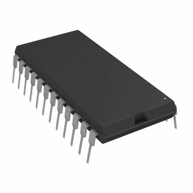
- Part No.:
- DS17485-5
- Manufacturer:
- Analog Devices Inc./Maxim Integrated
- Category:
- Real Time Clocks
- Package:
- 24-DIP (0.600", 15.24mm)
- Datasheet:
-
 DS17485-5.pdf
- Description:
- IC RTC CLK/CALENDAR PAR 24DIP
- Quantity:
- Payment:

- Shipping:

Inventory:2,534
Please send an inquiry. Send us your inquiry, and we will respond immediately.
Product details
Overview
The DS17485-5 from Maxim Integrated is a battery-backed real-time clock/calendar IC with 4096 bytes of NV SRAM, 114 bytes of general-purpose RAM, time-of-day alarm, six maskable interrupts, and programmable square-wave output. It operates at +3.0V or +5.0V, supports 12-/24-hour format with leap-year compensation through 2099, and integrates power-on control via PWR and KS pins for embedded system wake-up.
For engineers reviewing the DS17485-5 datasheet, DS17485-5 pinout, DS17485-5 application, or DS17485-5 equivalent, this page delivers verified timing accuracy (±1 min/month for EDIP variants), VCC/VBAT/VBAUX power-fail switching behavior, multiplexed AD0–AD7 bus interface timing, IRQ/SQW/PWR terminal functions, and industrial temperature support (–40°C to +85°C).
Technical Context
The DS17485-5 implements a fully autonomous RTC core with double-buffered time/calendar registers, automatic month-end and leap-year correction, and a 15-stage divider chain feeding a 13-tap programmable square-wave generator. Its power-control circuitry uses a precision temperature-compensated voltage reference to monitor VCC against VPF (4.25–4.5V @ 5V mode) and seamlessly switch to VBAT or VBAUX upon primary supply failure.
It features a multiplexed 8-bit address/data bus (AD0–AD7) with ALE-latched addressing, active-low RD/WR/CS controls, and open-drain IRQ/PWR outputs requiring external pullups. The device supports both crystal (X1/X2, 32.768kHz, 6pF or 12.5pF load) and external oscillator inputs, and includes a 64-bit silicon serial number and SMI recovery stack.
Key Specifications
| Parameter | Value and Actual Design Meaning |
|---|---|
| Supply Voltage | +2.7V to +3.7V or +4.5V to +5.5V - dual-voltage operation enables drop-in replacement in legacy 5V or modern 3V systems |
| RTC Accuracy | Factory-trimmed ±1 minute/month at 25°C (for DS17487 EDIP variant); DS17485-5 relies on external crystal matching |
| SRAM Capacity | 4096 bytes extended NV SRAM + 114 bytes general-purpose battery-backed RAM - retains data during main power loss |
| Interrupt Capability | Six independently maskable interrupt flags (AF, UF, PF, IRQF, etc.) sharing one open-drain IRQ output - simplifies host interrupt handling |
| Power-Fail Detection | VPF = 4.25–4.5V (5V mode) or 2.5–2.7V (3V mode) - triggers automatic switchover to backup supply without software intervention |
| Operating Temperature | –40°C to +85°C industrial range - qualified for utility meters, security systems, and network infrastructure |
| Crystal Interface | Supports 32.768kHz crystal with 6pF or 12.5pF load capacitance - selectable via crystal select bit; X1 accepts external oscillator |
Pinout & Package
DS17485-5 is available in 28-pin PDIP, SO, or TSOP packages. Pin count and function mapping match the DS17x85 family; no integrated crystal or battery (unlike DS17487 EDIP).
| Pin/Terminal | Circuit Role | Design Meaning |
|---|---|---|
| AD0–AD7 | Multiplexed Address/Data Bus | Bidirectional 8-bit bus latched by ALE falling edge; carries addresses first, then data - reduces PCB trace count vs. separate buses |
| CS, RD, WR, ALE | Control Inputs | Active-low chip-select, read/write strobes, and address latch enable - standard Intel-style parallel interface compatible with 8051/8086 derivatives |
| IRQ | Open-Drain Interrupt Output | Active-low shared interrupt signal; requires external pullup; asserts when enabled flag bits are set - supports wired-OR interrupt busing |
| PWR | Open-Drain Power-On Control | Drives external power supply enable; activated by wake-up alarm or KS kickstart; software-controllable after power-on - enables zero-power standby architectures |
| KS | Active-Low Kickstart Input | Triggers system power-on from VCC-off state when pulled low; requires VBAUX and ABE=1 - supports keyboard or sensor-initiated wake-up |
| VBAT / VBAUX | Backup Supply Inputs | VBAT powers RTC and RAM during VCC loss; VBAUX enables KS/wake-up and extends runtime - dual-battery flexibility improves reliability |
| SQW | Programmable Square-Wave Output | Configurable 1Hz–32kHz output (13 taps); enabled by SQWE/E32k bits - provides clock source for microcontrollers or logic circuits |
| X1 / X2 | Crystal Oscillator Terminals | X1 accepts 32.768kHz crystal or external oscillator; X2 is internal oscillator output - no external caps required for specified CL |
Key Features
| Feature | Design Value |
|---|---|
| Leap-Year Compensation | Automatic date adjustment through year 2099 - eliminates firmware calendar logic for embedded applications |
| Power-On Wake-Up Logic | Hardware-triggered PWR assertion from time alarm or KS input - enables energy-efficient always-on monitoring without MCU polling |
| Extended NV SRAM | 4096-byte battery-backed memory - stores configuration, logs, or calibration data across power cycles without EEPROM wear |
| 64-Bit Silicon Serial Number | Factory-programmed unique ID per unit - enables secure device authentication and inventory tracking in networked systems |
| VCC/VBAT/VBAUX Triple-Supply Management | Intelligent switchover with independent voltage thresholds - ensures continuous RTC operation even if primary or auxiliary supplies degrade |
Applications
| Smart Utility Metering | Industrial Security Panel |
|---|---|
Use Scenario: Time-stamped energy consumption logging and tamper-event recording in electricity/gas/water meters operating unattended for >10 years. IC Role / Device Role / Timing Role: Primary RTC and nonvolatile data logger; maintains accurate UTC time and stores metering history in 4096-byte NV SRAM. Use Value: Eliminates need for external EEPROM and RTC co-location; battery-backed retention meets ANSI C12.1/C12.20 compliance for 10+ year data integrity. | Use Scenario: Intrusion detection panel that wakes from deep sleep only upon scheduled arming/disarming or door/window sensor activation. IC Role / Device Role / Timing Role: System-level wake controller and time-source; generates IRQ on alarm time and asserts PWR to power up MCU and sensors. Use Value: Reduces average system current to <10 µA during standby - extends lithium battery life beyond 5 years in battery-only deployments. |
| Network Infrastructure Clock | Medical Device Timestamping |
Use Scenario: Time synchronization and event logging in Ethernet switches/routers where NTP is unavailable or unreliable. IC Role / Device Role / Timing Role: Standalone wall-clock reference with alarm-driven log rotation; SQW output drives watchdog or sampling clock. Use Value: Provides deterministic, drift-compensated timestamps independent of network stack - critical for forensic packet capture and audit trails. | Use Scenario: Patient monitor storing vital sign trends with precise timestamps during AC power loss or transport. IC Role / Device Role / Timing Role: Fail-safe timekeeper and data buffer; retains real-time clock and 114-byte RAM contents using coin-cell backup. Use Value: Guarantees continuity of clinical timestamps per IEC 62304 Class B requirements - prevents data gaps during power transitions. |
Equivalent & Alternatives
The following parts are listed as comparable options for similar real-time clock applications.
| Alternative Part | Technical Difference | Application Difference | Selection Advice |
|---|---|---|---|
| DS3231M | Integrated TCXO (±2ppm accuracy), I²C interface, no parallel bus or PWR/KS control | Lacks hardware wake-up capability and multiplexed bus; suited for space-constrained I²C designs | Choose DS3231M for highest accuracy and smallest footprint; avoid if PWR-controlled power gating or legacy parallel interface is required |
| PCF8583 | Legacy I²C RTC with 256-byte RAM, no alarm masking, no power-control outputs, max +70°C operation | No industrial temp support, no wake-up logic, limited interrupt flexibility | Choose PCF8583 only for cost-sensitive commercial-grade applications lacking wake-up or extended SRAM needs |
Compared with DS3231M and PCF8583, the DS17485-5 uniquely combines parallel bus compatibility, hardware-assisted system power control (PWR/KS), 4kB NV SRAM, and industrial temperature rating - making it irreplaceable in legacy-replacement and energy-gated embedded designs.
Availability
DS17485-5 is available at Aetrix Electronics and suitable for smart utility metering, industrial security panels, network infrastructure clocking, and medical timestamping requiring stable component supply across long product lifecycles.
Supply support for DS17485-5 includes scheduled delivery planning, volume procurement assistance, BOM continuity management, traceable sourcing, and lifecycle availability coordination for OEM customers, industrial embedded developers, connected-device designers, and electronics production programs.
Manufacturer
Maxim Integrated (now part of Analog Devices) designs high-performance analog and mixed-signal semiconductors for industrial, communications, and computing applications.
The DS17485-5 belongs to the DS17x85 RTC family, engineered to replace the DS12887 in systems needing enhanced SRAM, hardware wake-up, and robust power-fail management - targeting metering, security, and infrastructure equipment.
FAQ
What voltage options does the DS17485-5 support?
The DS17485-5 supports two operating voltage ranges: +2.7V to +3.7V and +4.5V to +5.5V. This dual-voltage capability allows direct integration into both modern 3V systems and legacy 5V designs without level-shifting. The DS17485-5 automatically detects the applied VCC range and configures internal regulators and thresholds accordingly - for example, VPF shifts from 2.5–2.7V in 3V mode to 4.25–4.5V in 5V mode. Both modes maintain full functionality including RTC, SRAM, and interrupt generation.
How does the DS17485-5 handle power failure and battery switchover?
The DS17485-5 uses a precision temperature-compensated comparator to continuously monitor VCC against the power-fail threshold (VPF). When VCC drops below VPF, the device immediately disables read/write access and switches power to the higher of VBAT or VBAUX - preserving RTC operation and SRAM contents. The DS17485-5 guarantees seamless transition with no time loss or register corruption. Recovery occurs after tREC (20–150ms) once VCC rises above VPF, ensuring stable initialization before host access resumes.
What is the role of the PWR and KS pins on the DS17485-5?
The PWR pin is an open-drain output used to control external power supplies; it activates automatically on wake-up alarm or KS input assertion, and remains software-controllable after boot. The KS (Kickstart) pin is an active-low input that triggers PWR assertion when VCC is absent - enabling hardware-initiated power-on from switches or sensors. For the DS17485-5, KS requires VBAUX and the auxiliary-battery-enable bit (ABE) set to 1. These pins together form a complete hardware power-gating solution, eliminating the need for external supervisors or discrete logic in battery-backed systems.
Does the DS17485-5 include an integrated crystal or battery?
No, the DS17485-5 does not integrate a crystal or battery. It is a bare-die RTC IC in PDIP/SO/TSOP packages requiring an external 32.768kHz crystal connected to X1/X2 (with 6pF or 12.5pF load capacitance) and a separate lithium coin cell on VBAT. This contrasts with the DS17487, which packages crystal and battery in a 24-pin EDIP module. The DS17485-5's discrete design allows board-level optimization of crystal layout, thermal management, and battery selection - critical for high-reliability metering and industrial applications.
What memory resources does the DS17485-5 provide?
The DS17485-5 provides three distinct memory regions: 114 bytes of general-purpose battery-backed RAM accessible via the AD0–AD7 bus; 4096 bytes of extended battery-backed NV SRAM (unique to DS17485/DS17487 variants); and 18 bytes of dedicated RTC/calendar/alarm registers. All memory retains data during VCC loss using VBAT or VBAUX. The extended SRAM is ideal for firmware parameter storage, event logs, or calibration tables - avoiding wear-prone EEPROM and enabling byte-level writes without erase cycles. The DS17485-5's RAM clear function (RCLR pin) allows secure erasure of user RAM without affecting RTC registers.
DS17485-5 Specifications
- Product attributes
- Attribute value
- Manufacturer:
- Analog Devices Inc./Maxim Integrated
- Series:
- -
- Package/Case:
- 24-DIP (0.600", 15.24mm)
- Packaging:
- Tube
- Product Status:
- Obsolete
- Programmable:
- Not Verified
- Type:
- Clock/Calendar
- Features:
- Alarm, Daylight Savings, Leap Year, NVSRAM, Square Wave Output
- Memory Size:
- 4KB
- Time Format:
- HH:MM:SS (12/24 hr)
- Date Format:
- YY-MM-DD-dd
- Interface:
- Parallel
- Voltage - Supply:
- 4.5V ~ 5.5V
- Voltage - Supply, Battery:
- 2.5V ~ 3.7V
- Current - Timekeeping (Max):
- 3mA @ 4.5V ~ 5.5V
- Operating Temperature:
- 0°C ~ 70°C
- Mounting Type:
- Through Hole
- Grade:
- -
- Qualification:
- -
- Supplier Device Package:
- 24-PDIP
DS17485-5 FAQ
1.How can I place an order for DS17485-5 through Aetrix?
Please submit a Request for Quotation (RFQ) for DS17485-5 on Aetrix. Our sales agent will provide a competitive quotation and guide you through the order confirmation once you accept the terms.
2.Are the price and stock information for DS17485-5 reliable?
The price and inventory of DS17485-5 are updated periodically and may fluctuate due to market conditions. Stock and pricing data are typically refreshed every 24 hours. Quotation validity for DS17485-5 is usually 5 days.
3.What payment methods are accepted for DS17485-5?
We accept Wire Transfer, PayPal, Credit Card, Western Union, MoneyGram, and Escrow for DS17485-5 transactions.
Note: Certain payment methods may incur a processing fee.
4.How is shipping managed for DS17485-5?
DS17485-5 orders can be shipped via leading logistics carriers, including DHL, UPS, FedEx, TNT, or Registered Mail.
Once your DS17485-5 order is processed, you will receive an email with the shipment details and tracking number.
Note: Tracking information may take up to 24 hours to appear. Express delivery typically takes 3–5 business days.
5.How can I obtain technical support or documentation for DS17485-5?
For technical support, including DS17485-5 datasheets, pinout diagrams, or application guidance, please contact our engineering support team. They can provide detailed documentation and assistance for your DS17485-5 requirements.
6.How does Aetrix verify that DS17485-5 is sourced from the original manufacturer or authorized distributors?
All DS17485-5 products on Aetrix are procured from qualified distributors and authorized channels. Our dedicated quality assurance team conducts strict verification, including traceability checks and, if necessary, third-party testing. This ensures that DS17485-5 meets industry standards.
7.What is the process for return or replacement of DS17485-5?
All DS17485-5 units undergo pre-shipment inspection (PSI). If there is an issue with DS17485-5, returns or replacements are accepted under the following conditions:
1.Quantity discrepancies, incorrect items, or visible external defects (such as breakage or corrosion), acknowledged by Aetrix.
2.The issue is reported within 90 days of delivery.
3.The DS17485-5 part is unused and in its original packaging.
Return procedure for DS17485-5:
1.Submit a request within 90 days.
2.Obtain a Return Material Authorization (RMA) from Aetrix.
DS17485-5 Tags

-
MCP7940N-I/SN
Microchip Technology
-
MCP7940MT-I/MNY
Microchip Technology

-
PCF85063ATL/1,118
NXP USA Inc.
-
MCP7940NT-I/SN
Microchip Technology

-
MCP7940NT-I/MS
Microchip Technology
-
MCP7940N-I/MS
Microchip Technology
-
PCF85063AT/AY
NXP USA Inc.

-
PCF85063TP/1Z
NXP Semiconductors

-
PCF85063ATT/AJ
NXP USA Inc.
-
MCP7940NT-E/SN
Microchip Technology
-
MCP7940NT-I/MNY
Microchip Technology
-
MCP79400T-I/SN
Microchip Technology
Tech Hub

A practical engineering guide to 3.3V and 5V logic compatibility, input thresholds, resistor dividers, translator ICs, MOSFET level shifting, I2C pull-ups, timing limits and power-sequencing risks.

The 74HC595 uses push-pull logic outputs, while the TPIC6B595 uses 50 V open-drain DMOS sinks for higher-power loads. This guide compares timing, current limits, 3.3 V interfacing, load wiring, thermal…

The 74HC595 converts serial data into eight stable parallel outputs. This guide covers pin functions, shift and storage timing, OE and MR behavior, drive-current limits, cascading, voltage compatibilit…

A technical comparison of level-sensitive latches and edge-triggered flip-flops, covering timing windows, setup and hold limits, master–slave operation, time borrowing, race-through, HDL inference and…

A D latch stores one bit while Enable controls when data can pass. This reference covers gate-level operation, truth tables, transparency, setup and hold timing, LE versus OE, common ICs and practical …

An SR latch stores one bit through cross-coupled feedback. This engineering reference covers NOR and NAND implementations, truth tables, forbidden-state recovery, gated operation, switch debouncing, fa…

Latch circuits retain one bit through feedback. This technical reference covers SR and D latches, truth tables, transparency, timing limits, latch-versus-flip-flop behavior, applications and common log…

An engineering guide to LED driver operation, constant-current and constant-voltage outputs, linear and switching topologies, dimming, IC selection, calculations, replacement compatibility, and fault c…

Operational amplifier guide covering op amp basics, feedback, ideal vs real op amps, common configurations, buffer circuits, offset, bias current, gain-bandwidth, slew rate, rail-to-rail limits and sel…

Jumper cables guide covering safe connection order, red and black clamp placement, final ground connection, cable gauge, length, clamp quality, copper vs CCA cables, jump starter comparison and battery…


