
 My Inquiry
 My Account


Analog Devices Inc./Maxim Integrated DS1852B-00C+T&R
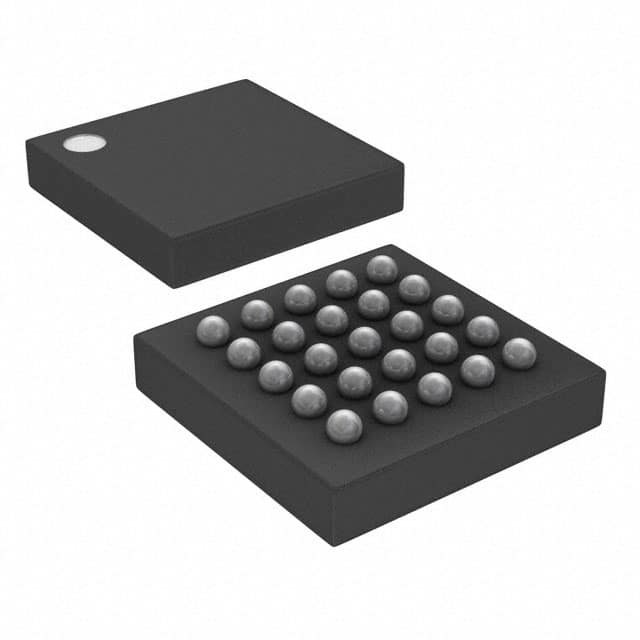
- Part No.:
- DS1852B-00C+T&R
- Manufacturer:
- Analog Devices Inc./Maxim Integrated
- Category:
- Specialized
- Package:
- 25-LFBGA, CSPBGA
- Datasheet:
-
 DS1852B-00C+T&R.pdf
- Description:
- IC INTERFACE SPECIALIZED 25BGA
- Quantity:
- Payment:

- Shipping:

Inventory:4,131
Please send an inquiry. Send us your inquiry, and we will respond immediately.
Product details
Overview
DS1852B-00C+T&R from Maxim Integrated is a fiber-optic transceiver diagnostic monitor IC implementing SFF-8472 at device address A2h, featuring a 4-input muxing ADC (12-bit effective resolution), direct-to-digital temperature sensor (−40°C to +100°C range), and three temperature-compensated fast comparators with <10µs response. It operates from 2.7V–5.5V and supports 2-wire interface for host communication in GBIC/SFP modules.
For engineers reviewing the DS1852B-00C+T&R datasheet, DS1852B-00C+T&R pinout, DS1852B-00C+T&R application, or DS1852B-00C+T&R equivalent, key selection criteria include SFF-8472 compliance readiness, on-chip EEPROM security levels (127/128 bytes), analog input scaling calibration per channel, and fast alarm trip point programmability across temperature ranges.
Technical Context
The DS1852B-00C+T&R integrates a 5-channel ADC (VCC, internal temp, Bin, Pin, Rin) with rotating 13ms nominal conversion cycle and 16-bit readout (12 MSBs valid). Each analog input supports independent 16-bit scaling calibration stored in Table 03h EEPROM (C8h–CFh), enabling full-scale adjustment from 0.2V to 6.5535V.
It implements dual-layer alarm architecture: ten high-resolution 16-bit alarm/warning comparators (set points in Table 03h) plus three temperature-dependent fast comparators (8-bit trip values, D8h–E7h) with eight unique trip points for Bin and four for Pin/Rin. All digital inputs (Din, RSin, Fin, Lin) are mirrored into Table 00h byte 6Eh.
Key Specifications
| Parameter | Value and Actual Design Meaning |
|---|---|
| Supply Voltage | 2.7V–5.5V operation enables compatibility with both 3V and 5V optical module power rails. |
| Operating Temp | −40°C to +100°C ambient range supports industrial-grade transceiver deployment in harsh environments. |
| ADC Resolution | 12-bit effective (16-bit read, LSBs undefined) provides 0.0039°C temp resolution and 38.147µV LSB for analog inputs. |
| Fast Comparator Speed | <10µs response time enables real-time fault detection for TX disable, LOS, and power-level events. |
| 2-Wire Interface | Supports standard (100kHz) and fast mode (400kHz) I²C protocols with open-drain SDA/SCL and ASEL-controlled addressing. |
| Security Levels | Three-tier access: User (read-only IEEE table), Manufacturer Level 1 (customer data), Level 2 (full memory control). |
| EEPROM Capacity | 127 bytes at Level 1, 128 bytes at Level 2 - sufficient for calibration coefficients, vendor ID, and alarm thresholds. |
Pinout & Package
Package: 25-ball BGA, 5mm × 5mm, 0.8mm pitch, lead-free (RoHS-compliant).
| Pin/Terminal | Circuit Role | Design Meaning |
|---|---|---|
| VCC (D2, D4, E3) | Power supply input | Multiple connections reduce IR drop and improve noise immunity for analog/digital sections. |
| GND (B3, C2, C4, D3) | Ground reference | Dedicated ground balls minimize ground bounce during fast comparator transitions. |
| SDA (B5) | 2-wire serial data | Open-drain output requires external pull-up; supports wire-OR with other I²C slaves. |
| SCL (A5) | 2-wire serial clock | Input only; synchronizes all I²C reads/writes and EEPROM programming cycles. |
| Bin (A3), Pin (D1), Rin (A2) | Analog monitor inputs | Direct connection to laser bias current, transmitted optical power, and received optical power signals. |
| ASEL (B2) | Address select | Logic-high configures device address to A2h (SFF-8472 default); logic-low sets to A0h. |
| Din (C5), RSin (B4), Fin (E5), Lin (A1) | Digital status inputs | Mirrored into Table 00h byte 6Eh for host polling of TX disable, rate select, TX fault, and LOS states. |
| NC (A4, B1, C1, D5, E1, E2, E4, C3) | No-connect | Unused balls - must be left unconnected per layout guidelines to avoid parasitic coupling. |
Key Features
| Feature | Design Value |
|---|---|
| Temperature-compensated fast comparators | Enables dynamic trip-point adjustment across −40°C to +100°C, preventing false alarms due to thermal drift in optical components. |
| Per-channel analog scaling calibration | 16-bit trim (4-bit coarse + 12-bit fine) in EEPROM allows precise full-scale matching for diverse photodiode and monitor diode transfer functions. |
| Three-tier security architecture | Prevents unauthorized overwrite of calibration data and vendor identity fields while allowing field updates to user-configurable alarm thresholds. |
| Integrated 2-wire interface with ACK polling | Enables reliable EEPROM write verification without host timing assumptions, critical for in-system calibration updates. |
| Simultaneous A/D monitoring of five parameters | Rotating 13ms update cycle ensures timely visibility into VCC, temperature, bias, transmit power, and receive power - all required by SFF-8472. |
Applications
| Fiber Channel Transceivers | SFP Modules |
|---|---|
Use Scenario: Real-time monitoring of laser bias current, transmitter output power, and receiver signal level in 1G/2G FC transceivers. IC Role / Device Role / Timing Role: Diagnostic monitor IC providing SFF-8472-compliant telemetry via 2-wire interface to host controller. Use Value: Enables closed-loop laser power control and early-warning fault detection using calibrated ADC and temperature-compensated comparators. | Use Scenario: Embedded diagnostics in hot-pluggable SFP modules for Ethernet switches and routers. IC Role / Device Role / Timing Role: Transceiver monitor managing EEPROM identity storage, analog sensing, and digital status mirroring per SFF-8472. Use Value: Reduces BOM count by integrating ADC, temp sensor, comparators, and secure EEPROM - eliminating need for discrete monitoring components. |
| GBIC Modules | Optical Line Cards |
Use Scenario: Compliance verification and performance tracking in legacy Gigabit Interface Converter modules. IC Role / Device Role / Timing Role: SFF-8472 proposal implementation engine with A2h device address and external A0h EEPROM support. Use Value: Ensures interoperability with host systems requiring standardized digital diagnostics, including vendor-specific calibration data storage. | Use Scenario: High-density optical line cards in telecom central offices requiring stable thermal management and fault isolation. IC Role / Device Role / Timing Role: Centralized analog/digital monitor for multiple transceiver lanes with shared 2-wire bus access. Use Value: Supports multi-lane synchronization via common clock domain and enables predictive maintenance using historical temperature and power trend logging. |
Equivalent & Alternatives
The following parts are listed as comparable options for similar transceiver monitor applications.
| Alternative Part | Technical Difference | Application Difference | Selection Advice |
|---|---|---|---|
| MAX32660GWE+T | ARM Cortex-M4F MCU with integrated ADC, temp sensor, and I²C; no native SFF-8472 memory map or fast comparators. | Requires firmware development for SFF-8472 compliance; suitable for custom diagnostics but not drop-in replacement. | Select when flexible programmability and future feature expansion outweigh SFF-8472 out-of-box compliance. |
| LM75BIMM/NOPB | Dedicated digital temperature sensor only; no ADC, comparators, EEPROM, or transceiver-specific registers. | Limited to thermal monitoring; cannot replace DS1852B-00C+T&R's full diagnostic functionality in optical modules. | Select only as supplemental temp sensor where primary monitoring is handled elsewhere. |
Compared with MAX32660GWE+T and LM75BIMM/NOPB, the DS1852B-00C+T&R delivers turnkey SFF-8472 compliance with calibrated multi-channel analog monitoring, hardware-accelerated alarm generation, and secure EEPROM - eliminating firmware development and reducing system validation effort for optical transceiver designs.
Availability
DS1852B-00C+T&R is available at Aetrix Electronics and suitable for fiber channel transceivers, SFP modules, GBIC modules, and optical line cards requiring stable component supply, long-term lifecycle support, and RoHS-compliant packaging.
Supply support for DS1852B-00C+T&R includes scheduled delivery planning, volume procurement assistance, BOM continuity management, traceable sourcing, and lifecycle availability coordination for OEM customers, industrial embedded developers, connected-device designers, and electronics production programs.
Manufacturer
Maxim Integrated (now part of Analog Devices) designs precision analog, mixed-signal, and power management ICs for industrial, communications, and computing applications.
The DS1852B-00C+T&R belongs to Maxim's optical transceiver monitor product line, engineered specifically to implement SFF-8472 diagnostics in pluggable fiber modules with minimal external components.
FAQ
What is the primary function of the DS1852B-00C+T&R in an optical transceiver?
The DS1852B-00C+T&R serves as a dedicated diagnostic monitor IC that implements SFF-8472 proposals for real-time monitoring of temperature, supply voltage, laser bias current (Bin), transmitted optical power (Pin), and received optical power (Rin). It provides calibrated analog-to-digital conversion, programmable alarm/warning thresholds, and secure EEPROM storage - all accessible via a 2-wire interface. The DS1852B-00C+T&R enables host systems to perform health monitoring, fault prediction, and compliance reporting without external support circuitry.
Does the DS1852B-00C+T&R require an external EEPROM to meet SFF-8472 compliance?
Yes - full SFF-8472 compliance requires an external EEPROM at device address A0h to store mandatory vendor identity, calibration, and specification data. The DS1852B-00C+T&R itself contains 127–128 bytes of internal EEPROM for security-level configuration and alarm settings, but the IEEE-defined identity table (bytes 00h–5Fh) must reside externally. The DS1852B-00C+T&R communicates with both internal and external EEPROMs over the same 2-wire bus using ASEL pin control.
How does the DS1852B-00C+T&R handle temperature compensation for its fast comparators?
The DS1852B-00C+T&R implements temperature-dependent trip points for its three fast comparators: Bin supports eight unique trip values across temperature ranges, while Pin and Rin each support four. These values are stored in Table 03h (addresses D8h–E7h) and automatically applied based on the measured die temperature. This eliminates manual recalibration and ensures consistent fault detection thresholds despite thermal drift in laser diodes and photodiodes - a core requirement for reliable DS1852B-00C+T&R operation in variable-temperature optical environments.
What are the security access levels supported by the DS1852B-00C+T&R, and how are they enforced?
The DS1852B-00C+T&R enforces three security levels via 32-bit password protection: User (default, read-only access to IEEE identity and monitoring registers), Manufacturer Level 1 (read/write to customer data tables), and Manufacturer Level 2 (full memory and configuration access). Passwords are written to Table 00h bytes 7Bh–7Eh and compared against factory-programmed values in protected EEPROM. Level 2 access grants authority over all memory, including Level 1 data - ensuring DS1852B-00C+T&R safeguards calibration integrity and vendor identity fields against unauthorized modification.
Can the DS1852B-00C+T&R operate from a 3.3V supply, and what are its voltage tolerance limits?
Yes - the DS1852B-00C+T&R operates from 2.7V to 5.5V, making it fully compatible with standard 3.3V optical module supplies. Its analog monitoring circuitry begins functioning predictably above the analog minimum voltage (between 2.7V and digital minimum), and full specifications are guaranteed at ≥2.7V. The DS1852B-00C+T&R also supports 5V operation, simplifying design reuse across legacy and modern transceiver platforms without level-shifting circuitry.
DS1852B-00C+T&R Specifications
- Product attributes
- Attribute value
- Manufacturer:
- Analog Devices Inc./Maxim Integrated
- Series:
- -
- Package/Case:
- 25-LFBGA, CSPBGA
- Packaging:
- Tape & Reel (TR)
- Product Status:
- Obsolete
- Applications:
- Monitors
- Interface:
- 2-Wire
- Voltage - Supply:
- 2.7V ~ 5.5V
- Supplier Device Package:
- 25-CSBGA (5x5)
- Grade:
- -
- Qualification:
- -
- Mounting Type:
- Surface Mount
DS1852B-00C+T&R FAQ
1.How can I place an order for DS1852B-00C+T&R through Aetrix?
Please submit a Request for Quotation (RFQ) for DS1852B-00C+T&R on Aetrix. Our sales agent will provide a competitive quotation and guide you through the order confirmation once you accept the terms.
2.Are the price and stock information for DS1852B-00C+T&R reliable?
The price and inventory of DS1852B-00C+T&R are updated periodically and may fluctuate due to market conditions. Stock and pricing data are typically refreshed every 24 hours. Quotation validity for DS1852B-00C+T&R is usually 5 days.
3.What payment methods are accepted for DS1852B-00C+T&R?
We accept Wire Transfer, PayPal, Credit Card, Western Union, MoneyGram, and Escrow for DS1852B-00C+T&R transactions.
Note: Certain payment methods may incur a processing fee.
4.How is shipping managed for DS1852B-00C+T&R?
DS1852B-00C+T&R orders can be shipped via leading logistics carriers, including DHL, UPS, FedEx, TNT, or Registered Mail.
Once your DS1852B-00C+T&R order is processed, you will receive an email with the shipment details and tracking number.
Note: Tracking information may take up to 24 hours to appear. Express delivery typically takes 3–5 business days.
5.How can I obtain technical support or documentation for DS1852B-00C+T&R?
For technical support, including DS1852B-00C+T&R datasheets, pinout diagrams, or application guidance, please contact our engineering support team. They can provide detailed documentation and assistance for your DS1852B-00C+T&R requirements.
6.How does Aetrix verify that DS1852B-00C+T&R is sourced from the original manufacturer or authorized distributors?
All DS1852B-00C+T&R products on Aetrix are procured from qualified distributors and authorized channels. Our dedicated quality assurance team conducts strict verification, including traceability checks and, if necessary, third-party testing. This ensures that DS1852B-00C+T&R meets industry standards.
7.What is the process for return or replacement of DS1852B-00C+T&R?
All DS1852B-00C+T&R units undergo pre-shipment inspection (PSI). If there is an issue with DS1852B-00C+T&R, returns or replacements are accepted under the following conditions:
1.Quantity discrepancies, incorrect items, or visible external defects (such as breakage or corrosion), acknowledged by Aetrix.
2.The issue is reported within 90 days of delivery.
3.The DS1852B-00C+T&R part is unused and in its original packaging.
Return procedure for DS1852B-00C+T&R:
1.Submit a request within 90 days.
2.Obtain a Return Material Authorization (RMA) from Aetrix.
DS1852B-00C+T&R Tags

-
NVT4857UKAZ
NXP Semiconductors

-
TCA8418RTWR
Texas Instruments

-
PCA9546APWR
Texas Instruments

-
MD0100N8-G
Microchip Technology

-
PCA9548APW,118
NXP Semiconductors

-
PCA9540BDP,118
NXP Semiconductors

-
PCA9548APWR
Texas Instruments

-
PCA9546APW,118
NXP Semiconductors

-
PTN3360DBS,518
NXP Semiconductors

-
PCA9546ABS,118
NXP Semiconductors

-
PCA9518PWR
Texas Instruments

-
PCA9545APW,118
NXP Semiconductors
Tech Hub

A practical engineering guide to 3.3V and 5V logic compatibility, input thresholds, resistor dividers, translator ICs, MOSFET level shifting, I2C pull-ups, timing limits and power-sequencing risks.

The 74HC595 uses push-pull logic outputs, while the TPIC6B595 uses 50 V open-drain DMOS sinks for higher-power loads. This guide compares timing, current limits, 3.3 V interfacing, load wiring, thermal…

The 74HC595 converts serial data into eight stable parallel outputs. This guide covers pin functions, shift and storage timing, OE and MR behavior, drive-current limits, cascading, voltage compatibilit…

A technical comparison of level-sensitive latches and edge-triggered flip-flops, covering timing windows, setup and hold limits, master–slave operation, time borrowing, race-through, HDL inference and…

A D latch stores one bit while Enable controls when data can pass. This reference covers gate-level operation, truth tables, transparency, setup and hold timing, LE versus OE, common ICs and practical …

An SR latch stores one bit through cross-coupled feedback. This engineering reference covers NOR and NAND implementations, truth tables, forbidden-state recovery, gated operation, switch debouncing, fa…

Latch circuits retain one bit through feedback. This technical reference covers SR and D latches, truth tables, transparency, timing limits, latch-versus-flip-flop behavior, applications and common log…

An engineering guide to LED driver operation, constant-current and constant-voltage outputs, linear and switching topologies, dimming, IC selection, calculations, replacement compatibility, and fault c…

Operational amplifier guide covering op amp basics, feedback, ideal vs real op amps, common configurations, buffer circuits, offset, bias current, gain-bandwidth, slew rate, rail-to-rail limits and sel…

Jumper cables guide covering safe connection order, red and black clamp placement, final ground connection, cable gauge, length, clamp quality, copper vs CCA cables, jump starter comparison and battery…


