
 My Inquiry
 My Account


Analog Devices Inc./Maxim Integrated DS1856B-002
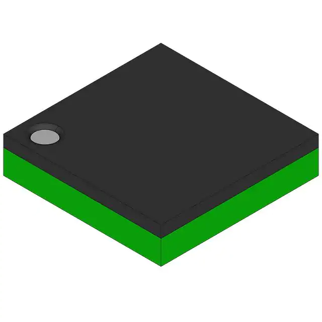
- Part No.:
- DS1856B-002
- Manufacturer:
- Analog Devices Inc./Maxim Integrated
- Category:
- Digital Potentiometers
- Package:
- 16-LBGA, CSPBGA
- Datasheet:
-
 DS1856B-002.pdf
- Description:
- DUAL TEMP-CONTROLLED RESISTOR
- Quantity:
- Payment:

- Shipping:

Inventory:2,683
Please send an inquiry. Send us your inquiry, and we will respond immediately.
Product details
Overview
DS1856B-002 from Maxim Integrated is a dual, temperature-controlled, nonvolatile variable resistor IC with integrated analog monitors (MON1–MON3), direct-to-digital temperature sensor, and password-protected 2-wire interface. It delivers precise bias voltage/current compensation in optical transceivers across -40°C to +95°C, featuring two 256-position linear resistors, five monitored channels (VCC, temp, MON1–MON3), and SFF-8472 compliance.
For engineers reviewing the DS1856B-002 datasheet, DS1856B-002 pinout, DS1856B-002 application, or DS1856B-002 equivalent, this page provides verified technical context, real-world use cases, validated alternatives, and supply-chain support for optical module design, industrial instrumentation, and RF power amplifier biasing.
Technical Context
The DS1856B-002 implements a temperature-indexed look-up table architecture where each of its two 256-position resistors is assigned a unique resistance value per 2°C increment over -40°C to +102°C. Its 12-bit ADC digitizes VCC (100µV/LSB) and three external analog inputs (38.147µV/LSB), updating all five monitored channels every 47–60ms in round-robin sequence.
It supports dual 2-wire slave addresses (A0h/A2h) via ADEN configuration, enabling memory-mapped compatibility with DS1852/DS1858/DS1859 families. Password protection enforces three access levels-User, Level 1, and Level 2-governing read/write permissions across 128-byte auxiliary EEPROM and main device tables including resistor LUTs (Tables 04/05) and alarm thresholds.
Key Specifications
| Parameter | Value and Actual Design Meaning |
|---|---|
| Resistor Resolution | 256 positions (00h–FFh), enabling fine-grained bias tuning in 2°C temperature steps |
| Temperature Sensor Accuracy | ±3.0°C over -40°C to +95°C - sufficient for closed-loop thermal compensation in laser diode control |
| Analog Monitor Resolution | 12-bit ADC with 38.147µV/LSB (MON1–MON3) and 100µV/LSB (VCC) - supports <0.5% FS accuracy after factory calibration |
| Supply Voltage Range | 2.85V to 5.5V - compatible with both 3.3V and 5V optical module power rails |
| 2-Wire Interface Speed | Standard mode (100kHz) and Fast mode (400kHz) - meets SFF-8472 timing for real-time diagnostics |
| EEPROM Endurance | 50,000 write cycles at +70°C - ensures long-term reliability for field-programmable resistor settings |
| Operating Temperature | -40°C to +95°C - qualified for industrial and telecom-grade optical transceiver environments |
Pinout & Package
DS1856B-002 is housed in a 16-ball CSBGA package (4mm × 4mm, 1.0mm pitch), optimized for high-density optical module PCB layouts with minimal footprint and thermal resistance.
| Pin/Terminal | Circuit Role | Design Meaning |
|---|---|---|
| SDA (Ball B2) | 2-wire serial data I/O | Open-drain bidirectional bus line supporting multi-drop configurations with pull-up to VCC |
| SCL (Ball A2) | 2-wire serial clock input | Master-generated clock synchronizing register reads/writes and EEPROM programming |
| OUT1 (Ball C3) | Open-drain buffer output | Asserts Tx-FAULT or system interrupt when monitored values exceed user-defined alarm limits |
| IN1 (Ball A1) | TTL/CMOS-compatible input | Drives OUT1 logic state; used for external fault signaling (e.g., LOS assertion) |
| OUT2 (Ball B1) | Open-drain buffer output | Independent second interrupt output, configurable for separate monitoring events |
| IN2 (Ball C2) | TTL/CMOS-compatible input | Drives OUT2; enables dual-channel diagnostic flagging without additional logic |
| L0 / H0 (Balls D2 / B3) | Resistor 0 low/high terminals | Connect to laser bias path; voltage range limited to GND–VCC, no polarity constraint |
| L1 / H1 (Balls B4 / A4) | Resistor 1 low/high terminals | Independent second bias network; supports differential or redundant control schemes |
| MON1–MON3 (Balls D3/D4/C4) | External analog monitor inputs | Accept 0–2.5V signals; internally calibrated with scalable dynamic range and offset correction |
| VCC (Ball A3) | Power supply | Supplies core logic, ADC, EEPROM, and buffers; decoupling capacitor required per layout guidelines |
| GND (Ball D1) | Ground reference | Common return for analog/digital domains; must be low-impedance connection to minimize noise coupling |
Key Features
| Feature | Design Value |
|---|---|
| SFF-8472 Compliance | Fully satisfies diagnostic monitoring requirements for GBIC/SFP modules, including Tx/Rx power, bias, temperature, and voltage reporting |
| Five Monitored Channels | Simultaneous real-time tracking of VCC, internal temperature, and three external analog inputs with independent alarm/warning flags |
| Temperature-Compensated Resistors | Each resistor's value changes automatically every 2°C using factory-calibrated look-up tables - eliminates manual thermal derating |
| Three-Level Password Protection | User (read-only monitoring), Level 1 (auxiliary EEPROM access), Level 2 (full configuration) - prevents unauthorized firmware or calibration tampering |
| Dual 2-Wire Slave Addresses | ADEN bit enables either single-address (A2h only) or dual-address (A0h/A2h) operation - simplifies integration into legacy SFF systems |
Applications
| Optical Transceivers | RF Power Amplifiers |
|---|---|
Use Scenario: Bias current and modulation voltage control in SFP+ and XFP optical modules operating across industrial temperature ranges. IC Role / Device Role / Timing Role: Dual NV resistor sets laser diode bias and modulator Vpi; temperature sensor triggers automatic gain compensation; MON1–MON3 monitor TEC voltage, photodiode current, and supply ripple. Use Value: Enables SFF-8472-compliant digital diagnostics while maintaining ±3% bias stability over -40°C to +95°C without external compensation circuitry. |
Use Scenario: Setting gate bias and drain supply trim in GaN/LDMOS RF power amplifiers for base station and radar applications. IC Role / Device Role / Timing Role: Resistor 0 adjusts gate voltage for quiescent current; Resistor 1 trims drain supply feedback; temperature sensor feeds back to PA thermal management loop. Use Value: Achieves <±0.5% output power variation over temperature by correlating resistor settings to on-die thermal readings - reduces need for lookup-table-based FPGA compensation. |
| Instrumentation & Industrial Controls | Diagnostic Monitoring Systems |
Use Scenario: Precision sensor excitation and signal conditioning in portable gas analyzers and pressure transmitters requiring stable reference voltages. IC Role / Device Role / Timing Role: Resistor 0 configures constant-current source for bridge sensors; Resistor 1 sets gain in instrumentation amplifier; MON2 monitors reference voltage drift. Use Value: Delivers <10ppm/°C effective TC via temperature-indexed resistor tables - outperforms discrete thermistor networks in size, cost, and calibration effort. |
Use Scenario: Real-time health monitoring of telecom infrastructure equipment including power supplies, cooling fans, and optical receivers. IC Role / Device Role / Timing Role: MON1 tracks +12V rail; MON2 monitors fan tachometer; MON3 reads thermistor voltage; OUT1 asserts system-level FAULT on any threshold violation. Use Value: Consolidates five analog monitoring functions and two programmable resistors into one 4mm × 4mm package - reduces BOM count and improves board-level diagnostic coverage. |
Equivalent & Alternatives
The following parts are listed as comparable options for similar dual temperature-compensated resistor applications.
| Alternative Part | Technical Difference | Application Difference | Selection Advice |
|---|---|---|---|
| DS1856E-002 | Same electrical specs and memory map, but in 16-pin TSSOP (5.0mm × 4.4mm) instead of 16-ball CSBGA | Preferred for prototyping and through-hole-compatible evaluation; less suitable for space-constrained optical modules | Select DS1856E-002 when board assembly uses reflow-compatible TSSOP or requires easier probe access during validation |
| DS1859-002 | Shares identical resistor architecture and monitor functionality, but lacks MON3 input and has different memory mapping (no ADEN=1 compatibility mode) | Used in legacy SFF-8472 designs where third analog monitor is unnecessary and DS1852 backward compatibility is not required | Choose DS1859-002 only if MON3 is unused and existing firmware does not rely on DS1852-style auxiliary memory mapping |
Compared with DS1856E-002 and DS1859-002, the DS1856B-002 uniquely combines CSBGA packaging for high-density optical modules, full SFF-8472 compliance with five monitored channels, and DS1852-compatible memory organization - making it the only option supporting both miniaturization and interoperability with established transceiver firmware stacks.
Availability
DS1856B-002 is available at Aetrix Electronics and suitable for optical transceivers, RF power amplifiers, instrumentation systems, and diagnostic monitoring equipment requiring stable component supply, long-term lifecycle support, and guaranteed traceable sourcing.
Supply support for DS1856B-002 includes scheduled delivery planning, volume procurement assistance, BOM continuity management, traceable sourcing, and lifecycle availability coordination for OEM customers, industrial embedded developers, connected-device designers, and electronics production programs.
Manufacturer
Maxim Integrated (now part of Analog Devices) is a semiconductor company specializing in precision analog, mixed-signal, and power management ICs for industrial, communications, and computing applications.
The DS1856B-002 belongs to Maxim's optical monitoring and control product line, designed specifically to meet SFF-8472 requirements for digital diagnostics in pluggable fiber-optic transceivers while integrating temperature compensation and secure configuration.
FAQ
What is the primary function of the DS1856B-002 in optical transceiver applications?
The DS1856B-002 serves as a dual, temperature-compensated bias controller and diagnostic monitor in SFP/XFP modules. It sets laser diode bias current and modulator voltage using its two nonvolatile resistors, while simultaneously measuring internal temperature, VCC, and up to three external analog signals (e.g., photodiode current, TEC voltage). Its SFF-8472 compliance ensures seamless integration with host system diagnostics, and the DS1856B-002's password-protected memory prevents unauthorized calibration changes in deployed systems.
How does the DS1856B-002 implement temperature compensation for its resistors?
The DS1856B-002 uses a factory-calibrated, temperature-indexed look-up table (LUT) architecture. Each of its two 256-position resistors is assigned a specific resistance value for every 2°C increment across -40°C to +102°C. The internal temperature sensor reads die temperature, and the device automatically selects the corresponding LUT entry to update resistor settings - eliminating manual compensation algorithms. This behavior is confirmed in the DS1856B-002 datasheet's "Variable Resistors" section and supported by typical characteristics plots showing resistance vs. temperature for positions 00h and FFh.
What are the key differences between DS1856B-002 and DS1856E-002?
The DS1856B-002 and DS1856E-002 share identical electrical specifications, memory map, and functional behavior - differing only in package type. The DS1856B-002 uses a 16-ball CSBGA (4mm × 4mm), optimized for high-density optical module PCBs, while the DS1856E-002 uses a 16-pin TSSOP (5.0mm × 4.4mm), better suited for prototyping and manual assembly. Both support the same ADEN configuration, password levels, and SFF-8472 features. The DS1856B-002's smaller footprint and lower thermal resistance make it preferred for production transceivers.
Does the DS1856B-002 support multiple device addressing on a shared 2-wire bus?
Yes, the DS1856B-002 supports dual 2-wire slave addressing via the ADEN (Address Enable) bit in Table 03, byte 89h. When ADEN = 0, it responds to both A0h (auxiliary EEPROM) and A2h (main device) addresses; when ADEN = 1, all memory-including the 128-byte auxiliary EEPROM-is mapped into Tables 00h/01h and accessed solely via A2h. This flexibility allows the DS1856B-002 to coexist with other SFF-8472 devices on the same bus and maintain compatibility with legacy DS1852 firmware that expects dual-address operation.
What level of accuracy does the DS1856B-002 provide for analog voltage monitoring?
The DS1856B-002 achieves 0.25% to 0.5% full-scale accuracy for VCC and MON1–MON3 inputs after factory calibration, with 12-bit resolution (38.147µV/LSB for MON inputs, 100µV/LSB for VCC). Input/Supply Offset is specified at 0–5 LSB, and update rate is 47–60ms per channel. These values are measured under recommended operating conditions (VCC = 2.85V–5.5V, TA = -40°C to +95°C) and documented in the "Analog Voltage Monitoring" section of the DS1856B-002 datasheet - confirming its suitability for precision bias and health monitoring tasks.
DS1856B-002 Specifications
- Product attributes
- Attribute value
- Manufacturer:
- Analog Devices Inc./Maxim Integrated
- Series:
- -
- Package/Case:
- 16-LBGA, CSPBGA
- Packaging:
- Bulk
- Product Status:
- Active
- Programmable:
- -
- Taper:
- Linear
- Configuration:
- Rheostat
- Number of Circuits:
- 2
- Number of Taps:
- 256
- Resistance (Ohms):
- 2.5k, 10k
- Interface:
- I2C
- Memory Type:
- Non-Volatile
- Voltage - Supply:
- 2.85V ~ 5.5V
- Features:
- Temperature Sensor
- Tolerance:
- -
- Temperature Coefficient (Typ):
- 50ppm/°C
- Mounting Type:
- Surface Mount
- Grade:
- -
- Qualification:
- -
- Supplier Device Package:
- 16-CSBGA (4x4)
- Operating Temperature:
- -40°C ~ 95°C
- Resistance - Wiper (Ohms) (Typ):
- -
DS1856B-002 FAQ
1.How can I place an order for DS1856B-002 through Aetrix?
Please submit a Request for Quotation (RFQ) for DS1856B-002 on Aetrix. Our sales agent will provide a competitive quotation and guide you through the order confirmation once you accept the terms.
2.Are the price and stock information for DS1856B-002 reliable?
The price and inventory of DS1856B-002 are updated periodically and may fluctuate due to market conditions. Stock and pricing data are typically refreshed every 24 hours. Quotation validity for DS1856B-002 is usually 5 days.
3.What payment methods are accepted for DS1856B-002?
We accept Wire Transfer, PayPal, Credit Card, Western Union, MoneyGram, and Escrow for DS1856B-002 transactions.
Note: Certain payment methods may incur a processing fee.
4.How is shipping managed for DS1856B-002?
DS1856B-002 orders can be shipped via leading logistics carriers, including DHL, UPS, FedEx, TNT, or Registered Mail.
Once your DS1856B-002 order is processed, you will receive an email with the shipment details and tracking number.
Note: Tracking information may take up to 24 hours to appear. Express delivery typically takes 3–5 business days.
5.How can I obtain technical support or documentation for DS1856B-002?
For technical support, including DS1856B-002 datasheets, pinout diagrams, or application guidance, please contact our engineering support team. They can provide detailed documentation and assistance for your DS1856B-002 requirements.
6.How does Aetrix verify that DS1856B-002 is sourced from the original manufacturer or authorized distributors?
All DS1856B-002 products on Aetrix are procured from qualified distributors and authorized channels. Our dedicated quality assurance team conducts strict verification, including traceability checks and, if necessary, third-party testing. This ensures that DS1856B-002 meets industry standards.
7.What is the process for return or replacement of DS1856B-002?
All DS1856B-002 units undergo pre-shipment inspection (PSI). If there is an issue with DS1856B-002, returns or replacements are accepted under the following conditions:
1.Quantity discrepancies, incorrect items, or visible external defects (such as breakage or corrosion), acknowledged by Aetrix.
2.The issue is reported within 90 days of delivery.
3.The DS1856B-002 part is unused and in its original packaging.
Return procedure for DS1856B-002:
1.Submit a request within 90 days.
2.Obtain a Return Material Authorization (RMA) from Aetrix.
DS1856B-002 Tags
-
MCP4018T-103E/LT
Microchip Technology
-
MCP4018T-503E/LT
Microchip Technology

-
MCP4011T-103E/SN
Microchip Technology
-
MCP4018T-104E/LT
Microchip Technology
-
MCP4017T-503E/LT
Microchip Technology
-
MCP4018T-502E/LT
Microchip Technology
-
MCP4017T-103E/LT
Microchip Technology

-
MCP4531T-103E/MF
Microchip Technology
-
MCP4021T-202E/SN
Microchip Technology

-
MCP4023T-103E/CH
Microchip Technology
-
MCP4022T-503E/CH
Microchip Technology

-
MCP4551T-502E/MS
Microchip Technology
Tech Hub

A practical engineering guide to 3.3V and 5V logic compatibility, input thresholds, resistor dividers, translator ICs, MOSFET level shifting, I2C pull-ups, timing limits and power-sequencing risks.

The 74HC595 uses push-pull logic outputs, while the TPIC6B595 uses 50 V open-drain DMOS sinks for higher-power loads. This guide compares timing, current limits, 3.3 V interfacing, load wiring, thermal…

The 74HC595 converts serial data into eight stable parallel outputs. This guide covers pin functions, shift and storage timing, OE and MR behavior, drive-current limits, cascading, voltage compatibilit…

A technical comparison of level-sensitive latches and edge-triggered flip-flops, covering timing windows, setup and hold limits, master–slave operation, time borrowing, race-through, HDL inference and…

A D latch stores one bit while Enable controls when data can pass. This reference covers gate-level operation, truth tables, transparency, setup and hold timing, LE versus OE, common ICs and practical …

An SR latch stores one bit through cross-coupled feedback. This engineering reference covers NOR and NAND implementations, truth tables, forbidden-state recovery, gated operation, switch debouncing, fa…

Latch circuits retain one bit through feedback. This technical reference covers SR and D latches, truth tables, transparency, timing limits, latch-versus-flip-flop behavior, applications and common log…

An engineering guide to LED driver operation, constant-current and constant-voltage outputs, linear and switching topologies, dimming, IC selection, calculations, replacement compatibility, and fault c…

Operational amplifier guide covering op amp basics, feedback, ideal vs real op amps, common configurations, buffer circuits, offset, bias current, gain-bandwidth, slew rate, rail-to-rail limits and sel…

Jumper cables guide covering safe connection order, red and black clamp placement, final ground connection, cable gauge, length, clamp quality, copper vs CCA cables, jump starter comparison and battery…


