
 My Inquiry
 My Account


Analog Devices Inc./Maxim Integrated DS1862B+
- Part No.:
- DS1862B+
- Manufacturer:
- Analog Devices Inc./Maxim Integrated
- Category:
- Laser Drivers
- Package:
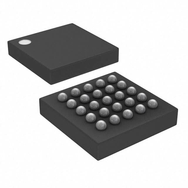
- 25-LFBGA, CSPBGA
- Datasheet:
-
 DS1862B+.pdf
- Description:
- IC LASR CTRLR 7CHAN 5.5V 25CSBGA
- Quantity:
- Payment:

- Shipping:

Inventory:2,362
Please send an inquiry. Send us your inquiry, and we will respond immediately.
Product details
Overview
The DS1862B+ from Maxim Integrated is a closed-loop laser-driver control IC with integrated digital diagnostics for XFP MSA-compliant 10Gbps optical transceiver modules. It implements automatic power control (APC), temperature-indexed extinction ratio control via lookup table (LUT), and monitors seven analog inputs-including bias monitor (IBIASMON), monitor diode current (BMD), RSSI, and dual auxiliary channels-for real-time laser regulation and safety fault detection.
For engineers reviewing the DS1862B+ datasheet, DS1862B+ pinout, DS1862B+ application, or DS1862B+ equivalent, this page delivers verified technical context, confirmed I²C interface timing (400kHz max), APC calibration accuracy (±5% over 0.2–1.5mA range), 25-ball CSBGA package mapping, and validated alternatives for XFP laser control systems requiring eye-safety quick-trip logic and EEPROM-stored calibration.
Technical Context
The DS1862B+ integrates a 13-bit ADC with round-robin multiplexing across seven monitored channels (five basic + two auxiliary), supporting factory- and user-calibrated gain/offset scaling per channel. Its APC loop dynamically adjusts BIASSET sink current to match photodiode feedback (BMD) against programmable register values, with loop bandwidth of 6–30kHz depending on IMD/IAPC ratio.
Extinction ratio control uses a 127-entry, temperature-indexed LUT stored in EEPROM; indexing is driven either by internal temperature sensor or external sensor on AUX2MON, with 2°C resolution across –40°C to +102°C. MODSET provides programmable sink current (0–1200μA) in five selectable ranges, while FETG enables external safety disconnect during fault conditions.
Key Specifications
| Parameter | Value and Actual Design Meaning |
|---|---|
| Main supply voltage | VCC3 = 2.9V to 5.5V - supports both 3.3V and 5V system rails without level-shifting |
| I²C clock frequency | Up to 400kHz - compatible with standard-mode I²C host controllers in XFP modules |
| APC calibration accuracy | ±5% over 0.200–1.5mA range at +25°C - ensures stable laser output power under thermal drift |
| Monitor update rate | 48–75ms frame time - configurable based on enabled channels (AUX1MON/AUX2MON disableable) |
| EEPROM endurance | 200k write cycles at +25°C - sufficient for field calibration updates and module reprogramming |
| Operating temperature | –40°C to +100°C - qualified for industrial-grade optical transceiver environments |
| Package | 25-ball CSBGA, 5mm × 5mm - surface-mount compatible with high-density XFP PCB layouts |
Pinout & Package
DS1862B+ is housed in a 25-ball Chip Scale Ball Grid Array (CSBGA) package measuring 5mm × 5mm, optimized for compact XFP module integration. Pin functions are validated per Maxim's official datasheet Rev 1 (12/07).
| Pin/Terminal | Circuit Role | Design Meaning |
|---|---|---|
| P-DOWN/RST (A1) | Power-down/reset input | Multifunction active-low pin with internal pullup; asserts hardware reset or initiates safe laser shutdown |
| BIASSET (C5) | Laser bias current sink output | Programmable current sink (0.01–1.50mA) driving laser anode; primary APC actuator |
| MODSET (B5) | Modulation current sink output | Sink-only output (0–1200μA) controlling laser cathode modulation; LUT-driven for extinction ratio |
| BMD (D5) | Monitor diode current interface | Configurable source/sink (±0.05–1.50mA); connects to photodiode for APC feedback and calibration |
| INTERRUPT (D1) | Open-drain fault indicator | Asserts on alarm/warning threshold breach (e.g., VCC2/3 fault, high bias, TX-P deviation) with 100ms delay |
| FETG (B3) | External FET gate driver | Drives external MOSFET for hardware-level laser safety disconnect during critical faults |
| SCL/SDA (B2/C2) | I²C serial interface | Standard-mode (400kHz) bidirectional bus; MOD-DESEL (E2) must be pulled low to enable communication |
Key Features
| Feature | Design Value |
|---|---|
| XFP MSA compliance | Fully implements digital diagnostics, serial ID, and user memory requirements per XFP Multi-Source Agreement |
| Seven-channel analog monitoring | Simultaneous measurement of temperature, VCC2/VCC3, BMD, RSSI, IBIASMON, AUX1MON, AUX2MON with 13-bit resolution |
| Internal calibration engine | Independent gain/offset registers per channel; factory-trimmed accuracy of ±0.25–0.5%FS for voltage inputs |
| Programmable quick-trip logic | Dedicated hardware path to disable laser within 30μs on safety-critical faults (e.g., overtemperature, overcurrent) |
| Password-protected EEPROM | Stores calibration data, LUT, thresholds, and configuration; prevents unauthorized modification in deployed modules |
Applications
| 10Gbps XFP Transceivers | Laser Safety-Critical Systems |
|---|---|
Use Scenario: High-speed optical links in telecom access networks and enterprise datacom requiring SFP+/XFP form factor compliance. IC Role / Device Role / Timing Role: Primary laser controller performing closed-loop APC, extinction ratio tuning, and real-time diagnostic reporting via I²C. Use Value: Enables stable 10Gbps operation across –40°C to +100°C with <±5% APC accuracy and automated LUT-based temperature compensation. |
Use Scenario: Optical modules deployed in unattended infrastructure where laser emission must comply with Class 1 eye-safety standards. IC Role / Device Role / Timing Role: Safety monitor enforcing hardware-level shutdown via FETG and P-DOWN/RST on fault detection (e.g., BMD >2.52mA). Use Value: Achieves <30μs laser disablement on critical faults, satisfying IEC 60825-1 safety response timing requirements. |
| Field-Programmable Optical Modules | Multi-Vendor Interoperable Transceivers |
Use Scenario: OEM transceiver modules requiring post-manufacturing calibration and firmware updates in depot or field. IC Role / Device Role / Timing Role: Host-accessible diagnostic hub storing calibrated coefficients, LUT entries, and alarm thresholds in password-protected EEPROM. Use Value: Supports up to 200k EEPROM write cycles at +25°C, enabling repeated recalibration without hardware replacement. |
Use Scenario: Datacenter switches sourcing XFP modules from multiple vendors needing consistent digital diagnostic behavior. IC Role / Device Role / Timing Role: XFP MSA-compliant interface providing standardized memory map (Table 01h–05h), I²C command set, and flag definitions. Use Value: Ensures interoperability with host controllers expecting MSA-defined register layout, interrupt semantics, and MOD-NR signaling. |
Equivalent & Alternatives
The following parts are listed as comparable options for similar laser control and digital diagnostic applications.
| Alternative Part | Technical Difference | Application Difference | Selection Advice |
|---|---|---|---|
| MAX32664A+T | Integrated ARM Cortex-M0+ MCU with optical diagnostics firmware; lacks dedicated APC loop and LUT-based extinction ratio control | Requires host firmware development for closed-loop control; better suited for custom diagnostics than drop-in XFP replacement | Select when full programmability and sensor fusion are needed over MSA compliance |
| ADN2880ACPZ-R7 | Single-channel 10Gbps limiting amplifier with LOS detection only; no laser bias/modulation control, no EEPROM, no APC/LUT functionality | Used only for receiver-side signal conditioning-not a functional substitute for transmitter laser control | Select only for RX-side signal integrity enhancement, not as a DS1862B+ alternative |
Compared with MAX32664A+T and ADN2880ACPZ-R7, the DS1862B+ uniquely delivers MSA-compliant, hardware-accelerated APC + LUT extinction ratio control in a single chip-enabling direct replacement in XFP modules without host software changes or external DACs.
Availability
DS1862B+ is available at Aetrix Electronics and suitable for 10Gbps optical transceivers, laser safety subsystems, and field-programmable XFP modules requiring stable component supply, long-term lifecycle support, and RoHS-compliant packaging.
Supply support for DS1862B+ includes scheduled delivery planning, volume procurement assistance, BOM continuity management, traceable sourcing, and lifecycle availability coordination for OEM customers, industrial embedded developers, connected-device designers, and electronics production programs.
Manufacturer
Maxim Integrated (now part of Analog Devices) designs precision analog, mixed-signal, and power management ICs for demanding industrial, communications, and computing applications.
The DS1862B+ belongs to Maxim's optical communications product line, engineered specifically to meet XFP MSA digital diagnostic requirements while integrating closed-loop laser control, safety monitoring, and EEPROM-based configuration storage.
FAQ
What is the primary function of the DS1862B+ in an XFP module?
The DS1862B+ serves as the core laser driver and digital diagnostic controller in XFP modules. It performs automatic power control (APC) by regulating BIASSET current to maintain constant optical output, implements temperature-compensated extinction ratio control using a 127-entry lookup table, and monitors seven analog signals-including BMD, RSSI, and VCC rails-to enforce safety thresholds and report diagnostics via I²C. Its design directly satisfies XFP MSA requirements for closed-loop control and real-time monitoring.
Does the DS1862B+ support both internal and external temperature sensing for LUT indexing?
Yes, the DS1862B+ supports both internal temperature sensing and external temperature sensing via the AUX2MON pin for LUT indexing. The internal sensor is always active and controls temperature-related alarm flags. When TEMP_INT/EXT = 1 (bit in Table 04h, Byte 8Bh), AUX2MON takes over LUT indexing-enabling precise extinction ratio tuning using an external thermistor or diode sensor-while the internal sensor continues monitoring for safety flag generation. This dual-path capability ensures robust thermal management in diverse module designs.
How does the DS1862B+ ensure laser eye safety compliance?
The DS1862B+ enforces laser eye safety through three hardware-verified mechanisms: (1) Quick-trip logic that disables laser bias within 30μs of detecting overtemperature, overcurrent, or over-optical-power faults; (2) FETG output capable of driving an external MOSFET to physically disconnect the laser; and (3) P-DOWN/RST pin that triggers full hardware reset. All paths operate independently of I²C communication, ensuring fail-safe behavior even during host processor lockup. These features align with IEC 60825-1 Class 1 safety requirements for optical transceivers.
What are the key electrical characteristics of the DS1862B+ I²C interface?
The DS1862B+ I²C interface operates in standard mode with a maximum clock frequency of 400kHz, matching common host controller capabilities in XFP systems. It features open-drain SDA/SCL pins with internal pullups (9–15kΩ), VIH ≥ 0.7×VCC3, VIL ≤ 0.3×VCC3, and tSU:DAT ≥ 100ns setup time. Communication requires MOD-DESEL (E2) to be pulled low first. EEPROM writes take 16ms per 4-byte block, and all register accesses follow XFP MSA-defined memory map (Tables 01h–05h), ensuring interoperability across vendor platforms.
Can the DS1862B+ monitor both VCC2 and VCC3 supply rails simultaneously?
No, the DS1862B+ monitors either VCC2 or VCC3-not both simultaneously. The selection is made via configuration bits in Table 04h, allowing users to choose which rail to measure for supply fault detection. VCC2 (1.6–3.6V) supports optional variable-supply XFP features, while VCC3 (2.9–5.5V) powers the main logic and analog blocks. If VCC2 is unused, it must be tied to VCC3 per datasheet Note 2. The monitored rail's voltage is digitized with 1.6mV resolution and ±0.25–0.5%FS accuracy after internal calibration.
DS1862B+ Specifications
- Product attributes
- Attribute value
- Manufacturer:
- Analog Devices Inc./Maxim Integrated
- Series:
- -
- Package/Case:
- 25-LFBGA, CSPBGA
- Packaging:
- Product Status:
- Obsolete
- Type:
- Laser Diode Controller (Fiber Optic)
- Data Rate:
- 10Gbps
- Number of Channels:
- 7
- Voltage - Supply:
- 2.9V ~ 5.5V
- Current - Supply:
- 3 mA
- Current - Modulation:
- -
- Current - Bias:
- -
- Operating Temperature:
- -40°C ~ 100°C
- Grade:
- -
- Qualification:
- -
- Supplier Device Package:
- 25-CSBGA (5x5)
- Mounting Type:
- Surface Mount
DS1862B+ FAQ
1.How can I place an order for DS1862B+ through Aetrix?
Please submit a Request for Quotation (RFQ) for DS1862B+ on Aetrix. Our sales agent will provide a competitive quotation and guide you through the order confirmation once you accept the terms.
2.Are the price and stock information for DS1862B+ reliable?
The price and inventory of DS1862B+ are updated periodically and may fluctuate due to market conditions. Stock and pricing data are typically refreshed every 24 hours. Quotation validity for DS1862B+ is usually 5 days.
3.What payment methods are accepted for DS1862B+?
We accept Wire Transfer, PayPal, Credit Card, Western Union, MoneyGram, and Escrow for DS1862B+ transactions.
Note: Certain payment methods may incur a processing fee.
4.How is shipping managed for DS1862B+?
DS1862B+ orders can be shipped via leading logistics carriers, including DHL, UPS, FedEx, TNT, or Registered Mail.
Once your DS1862B+ order is processed, you will receive an email with the shipment details and tracking number.
Note: Tracking information may take up to 24 hours to appear. Express delivery typically takes 3–5 business days.
5.How can I obtain technical support or documentation for DS1862B+?
For technical support, including DS1862B+ datasheets, pinout diagrams, or application guidance, please contact our engineering support team. They can provide detailed documentation and assistance for your DS1862B+ requirements.
6.How does Aetrix verify that DS1862B+ is sourced from the original manufacturer or authorized distributors?
All DS1862B+ products on Aetrix are procured from qualified distributors and authorized channels. Our dedicated quality assurance team conducts strict verification, including traceability checks and, if necessary, third-party testing. This ensures that DS1862B+ meets industry standards.
7.What is the process for return or replacement of DS1862B+?
All DS1862B+ units undergo pre-shipment inspection (PSI). If there is an issue with DS1862B+, returns or replacements are accepted under the following conditions:
1.Quantity discrepancies, incorrect items, or visible external defects (such as breakage or corrosion), acknowledged by Aetrix.
2.The issue is reported within 90 days of delivery.
3.The DS1862B+ part is unused and in its original packaging.
Return procedure for DS1862B+:
1.Submit a request within 90 days.
2.Obtain a Return Material Authorization (RMA) from Aetrix.
DS1862B+ Tags
-
EPC21701
EPC
-
EPC21601
EPC
-
MAX3799ETJ+T
Analog Devices Inc./Maxim Integrated
-
AD9665ACPZ-REEL7
Analog Devices Inc.

-
MAX3740AETG+T
Analog Devices Inc./Maxim Integrated
-
MAX3795ETG+
Analog Devices Inc./Maxim Integrated

-
EPC21603
EPC
-
ONET8501VRGPT
Texas Instruments
-
MAX3738ETG+T
Analog Devices Inc./Maxim Integrated
-
SY88022ALMG-TR
Microchip Technology
-
ISL78365ARZ-T7A
Renesas
-
EPC21603ENGRT
EPC
Tech Hub

A practical engineering guide to 3.3V and 5V logic compatibility, input thresholds, resistor dividers, translator ICs, MOSFET level shifting, I2C pull-ups, timing limits and power-sequencing risks.

The 74HC595 uses push-pull logic outputs, while the TPIC6B595 uses 50 V open-drain DMOS sinks for higher-power loads. This guide compares timing, current limits, 3.3 V interfacing, load wiring, thermal…

The 74HC595 converts serial data into eight stable parallel outputs. This guide covers pin functions, shift and storage timing, OE and MR behavior, drive-current limits, cascading, voltage compatibilit…

A technical comparison of level-sensitive latches and edge-triggered flip-flops, covering timing windows, setup and hold limits, master–slave operation, time borrowing, race-through, HDL inference and…

A D latch stores one bit while Enable controls when data can pass. This reference covers gate-level operation, truth tables, transparency, setup and hold timing, LE versus OE, common ICs and practical …

An SR latch stores one bit through cross-coupled feedback. This engineering reference covers NOR and NAND implementations, truth tables, forbidden-state recovery, gated operation, switch debouncing, fa…

Latch circuits retain one bit through feedback. This technical reference covers SR and D latches, truth tables, transparency, timing limits, latch-versus-flip-flop behavior, applications and common log…

An engineering guide to LED driver operation, constant-current and constant-voltage outputs, linear and switching topologies, dimming, IC selection, calculations, replacement compatibility, and fault c…

Operational amplifier guide covering op amp basics, feedback, ideal vs real op amps, common configurations, buffer circuits, offset, bias current, gain-bandwidth, slew rate, rail-to-rail limits and sel…

Jumper cables guide covering safe connection order, red and black clamp placement, final ground connection, cable gauge, length, clamp quality, copper vs CCA cables, jump starter comparison and battery…


