
 My Inquiry
 My Account


Analog Devices Inc./Maxim Integrated DS1867S-100
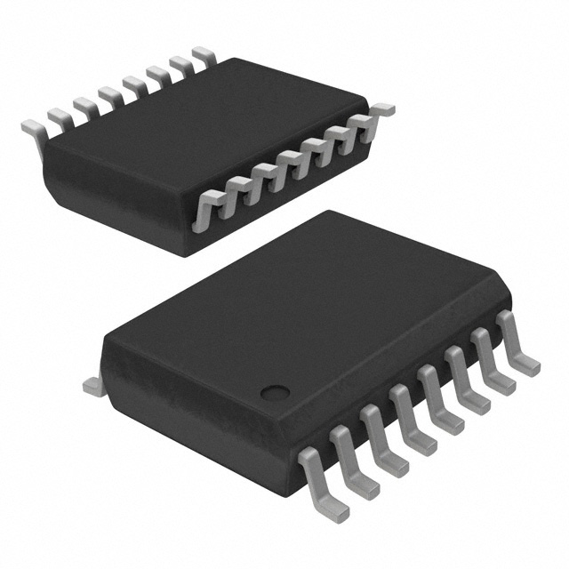
- Part No.:
- DS1867S-100
- Manufacturer:
- Analog Devices Inc./Maxim Integrated
- Category:
- Digital Potentiometers
- Package:
- 16-SOIC (0.295", 7.50mm Width)
- Datasheet:
-
 DS1867S-100.pdf
- Description:
- IC DGT POT 100KOHM 256TAP 16SOIC
- Quantity:
- Payment:

- Shipping:

Inventory:1,082
Please send an inquiry. Send us your inquiry, and we will respond immediately.
Product details
Overview
DS1867S-100 from Maxim Integrated (now Analog Devices) is a dual-channel, nonvolatile digital potentiometer with 256-position resolution per channel, 100 kΩ end-to-end resistance, EEPROM wiper storage, and 3-wire serial interface. It replaces mechanical trimmers in precision gain/attenuation circuits requiring power-loss immunity, such as programmable amplifier feedback networks and sensor calibration loops.
For engineers reviewing the DS1867S-100 datasheet, DS1867S-100 pinout, DS1867S-100 application, or DS1867S-100 equivalent, key selection considerations include its ±0.75 LSB absolute linearity, 100 kHz -3 dB bandwidth at 100 kΩ, industrial temperature range (-40°C to +85°C), and cascading capability for multi-device control over a single bus.
Technical Context
The DS1867S-100 implements two independent 8-bit-controlled resistive dividers with EEPROM-backed wiper positions stored during power-down via automatic 4 ms VCC trip-point detection (3.9–4.5 V). Its 3-wire serial port (RST/CLK/DQ) drives a 17-bit shift register containing wiper-0, wiper-1, and stack-select bits - enabling stacked or cascaded configurations without external logic.
Stacked mode connects H0–L1 internally to double total resistance to 200 kΩ while preserving 256-step resolution per pot; cascade mode uses COUT-to-DQ daisy-chaining with ≤70 ns propagation delay, supporting up to 17 × N-bit transfers across multiple devices on one bus.
Key Specifications
| Parameter | Value and Actual Design Meaning |
|---|---|
| Resistance Value | 100 kΩ ±20% end-to-end per potentiometer; sets maximum analog signal attenuation/gain range. |
| Wiper Resolution | 256 positions (8-bit); enables 0.39% incremental adjustment step size for fine-tuning. |
| Absolute Linearity | ±0.75 LSB typical; ensures voltage output deviation ≤ ±0.75 × (VCC/512) across full wiper sweep. |
| -3 dB Bandwidth | 100 kHz at 100 kΩ; defines usable AC signal frequency limit before gain drops 3 dB. |
| EEPROM Endurance | 25,000 write cycles; supports repeated field calibration without premature wear-out. |
| Supply Voltage | 4.5 V to 5.5 V; compatible with standard 5 V logic rails and tolerant of ±10% regulation. |
| Operating Temp | -40°C to +85°C; qualified for industrial environments including motor control and instrumentation. |
Pinout & Package
DS1867S-100 is packaged in 16-pin SOIC (300-mil), with pin 1 = VB, pin 16 = VCC. Pin functions are electrically validated per Maxim's DS1867 datasheet Rev 102199.
| Pin/Terminal | Circuit Role | Design Meaning |
|---|---|---|
| VB | Substrate bias | Enables operation with ±5 V supplies; must be tied to GND for single 5 V use. |
| H0, H1 | Potentiometer high ends | Fixed terminals defining top of each 100 kΩ resistive ladder; connect to reference voltage or amplifier input. |
| L0, L1 | Potentiometer low ends | Fixed terminals defining bottom of each ladder; typically grounded or connected to signal return. |
| W0, W1 | Wiper outputs | Variable tap points delivering adjustable voltage division; drive high-impedance nodes to minimize wiper resistance error (400–1000 Ω). |
| SOUT | Stacked wiper output | Multiplexed output of W0/W1 selected by stack bit; used only when potentiometers are series-connected for 200 kΩ operation. |
| RST, CLK, DQ | 3-wire serial interface | Asynchronous control: RST enables communication, CLK clocks data, DQ carries bidirectional 17-bit register writes/reads. |
| COUT | Cascade output | Drives DQ of next DS1867 in daisy chain; enables single-processor control of multiple units with 70 ns propagation delay. |
| VCC, GND | Power supply | 5 V ±10% supply with 250–900 µA active current; standby draws ≤250 µA. |
Key Features
| Feature | Design Value |
|---|---|
| Nonvolatile wiper storage | EEPROM retains last wiper position across power cycles without backup battery or external memory. |
| Stacked configuration support | Two 100 kΩ pots can be series-connected to yield 200 kΩ total resistance with same 256-step resolution. |
| Cascadable 3-wire interface | Single microcontroller GPIOs control unlimited DS1867S-100 units via COUT→DQ daisy chain with deterministic timing. |
| Industrial temperature rating | Guaranteed operation from -40°C to +85°C supports deployment in factory automation and outdoor equipment. |
| Low-power pumpless design | No internal charge pump eliminates switching noise and EMI, critical for precision analog signal paths. |
Applications
| Inverting Variable-Gain Amplifier | Fixed-Gain Signal Attenuator |
|---|---|
Use Scenario: Programmable gain stage in audio preamplifiers or sensor signal conditioning where gain must be set digitally and retained after power-off. IC Role / Device Role / Timing Role: Dual potentiometer provides feedback network for op-amp; W0 controls gain via Av = –n/(255–n), while W1 sets offset or secondary path. Use Value: Eliminates manual trimming; gain remains stable across thermal cycles and power interruptions due to EEPROM wiper retention. | Use Scenario: Precision attenuation of analog sensor outputs (e.g., thermocouple, RTD) prior to ADC sampling in industrial data loggers. IC Role / Device Role / Timing Role: Acts as digitally adjustable voltage divider; L0/GND and H0/VREF define attenuation ratio; W0 delivers scaled output to ADC input. Use Value: Enables field calibration compensation without hardware changes; 100 kΩ value minimizes loading on high-Z sensor sources. |
| Multi-Channel Calibration Module | Stacked High-Range Potentiometer |
Use Scenario: Modular calibration board for test equipment requiring independent adjustment of gain, offset, and reference levels across four channels. IC Role / Device Role / Timing Role: One DS1867S-100 per dual-channel section; serial interface allows microcontroller to update all pots synchronously via shared RST/CLK/DQ lines. Use Value: Reduces BOM count vs. discrete pots; EEPROM ensures calibrated settings survive firmware updates and cold starts. | Use Scenario: Replacement for 200 kΩ mechanical potentiometers in legacy industrial controllers where space and reliability are constrained. IC Role / Device Role / Timing Role: H0–L1 connection forms series stack; SOUT delivers combined wiper output; stack-select bit chooses W0 or W1 as active tap. Use Value: Delivers 200 kΩ range with 256-step resolution in same SOIC footprint; avoids redesigning PCB for larger package. |
Equivalent & Alternatives
The following parts are listed as comparable options for similar dual digital potentiometer applications.
| Alternative Part | Technical Difference | Application Difference | Selection Advice |
|---|---|---|---|
| AD5232BRUZ100 | 2.7–5.5 V supply; SPI interface; 1024-step resolution; no stacked mode; 20 kΩ wiper resistance. | Higher resolution but wider wiper resistance variation; requires SPI controller instead of 3-wire. | Select AD5232BRUZ100 if higher precision and SPI infrastructure exist; avoid if cascading or stacked resistance needed. |
| MCP42100-E/SL | 2.7–5.5 V supply; SPI interface; volatile RAM-only wiper storage; no EEPROM; 100 kΩ; 256 steps. | Requires external nonvolatile storage or initialization at boot; lacks power-loss retention. | Select MCP42100-E/SL only for cost-sensitive, always-powered systems where wiper reset on startup is acceptable. |
Compared with DS1867S-100, AD5232BRUZ100 offers finer resolution but lacks stacking and cascading; MCP42100-E/SL reduces cost and complexity but forfeits nonvolatility - making DS1867S-100 uniquely suited for unattended, field-calibrated analog systems requiring guaranteed post-power-up state.
Availability
DS1867S-100 is available at Aetrix Electronics and suitable for industrial instrumentation, sensor calibration modules, programmable gain amplifiers, and embedded test equipment requiring stable component supply and long-term parametric consistency.
Supply support for DS1867S-100 includes scheduled delivery planning, volume procurement assistance, BOM continuity management, traceable sourcing, and lifecycle availability coordination for OEM customers, industrial embedded developers, connected-device designers, and electronics production programs.
Manufacturer
Maxim Integrated (acquired by Analog Devices in 2021) designs precision analog and mixed-signal ICs for industrial, automotive, and communications markets.
The DS1867S-100 belongs to Maxim's digital potentiometer family targeting replacement of electromechanical trimmers in calibration-critical systems where power-loss resilience and serial configurability are mandatory.
FAQ
What is the supply voltage range for the DS1867S-100?
The DS1867S-100 operates from a single 4.5 V to 5.5 V supply. It also supports ±5 V operation when substrate bias (VB) is set to –5 V. The device includes an internal power-trip circuit that triggers EEPROM wiper storage when VCC falls below 4.5 V, ensuring reliable nonvolatile retention across brownout conditions.
Does the DS1867S-100 require an external clock source or charge pump?
No, the DS1867S-100 uses a pumpless architecture and requires only the externally provided CLK signal from the host controller. Its 3-wire serial interface (RST/CLK/DQ) operates without internal clock generation or charge pumps, eliminating switching noise and simplifying layout in noise-sensitive analog signal chains.
How does the DS1867S-100 retain wiper settings during power loss?
The DS1867S-100 retains wiper positions using on-chip EEPROM memory. When VCC drops below 4.5 V, the device automatically initiates a 4 ms wiper storage sequence, writing the current 17-bit I/O register contents to EEPROM. This occurs transparently without host intervention and supports ≥25,000 write cycles.
Can multiple DS1867S-100 devices share one serial bus?
Yes, DS1867S-100 devices support daisy-chain cascading via the COUT-to-DQ connection. Each device passes shifted data downstream with ≤70 ns propagation delay, allowing a single microcontroller to configure dozens of units using only three GPIOs (RST/CLK/DQ) and minimal additional wiring.
What is the function of the SOUT pin on the DS1867S-100?
The SOUT pin on the DS1867S-100 delivers the multiplexed wiper output of either potentiometer-0 (W0) or potentiometer-1 (W1), selected by bit-0 (stack select) of the 17-bit I/O shift register. It is used exclusively in stacked configuration where H0 and L1 are connected to form a 200 kΩ ladder, enabling single-point access to the combined wiper.
DS1867S-100 Specifications
- Product attributes
- Attribute value
- Manufacturer:
- Analog Devices Inc./Maxim Integrated
- Series:
- -
- Package/Case:
- 16-SOIC (0.295", 7.50mm Width)
- Packaging:
- Tube
- Product Status:
- Obsolete
- Programmable:
- Not Verified
- Taper:
- Linear
- Configuration:
- Potentiometer
- Number of Circuits:
- 2
- Number of Taps:
- 256
- Resistance (Ohms):
- 100k
- Interface:
- Serial
- Memory Type:
- Non-Volatile
- Voltage - Supply:
- 5V
- Features:
- Cascade Pin
- Tolerance:
- ±20%
- Temperature Coefficient (Typ):
- 750ppm/°C
- Mounting Type:
- Surface Mount
- Grade:
- -
- Qualification:
- -
- Supplier Device Package:
- 16-SOIC
- Operating Temperature:
- -40°C ~ 85°C
- Resistance - Wiper (Ohms) (Typ):
- 400
DS1867S-100 FAQ
1.How can I place an order for DS1867S-100 through Aetrix?
Please submit a Request for Quotation (RFQ) for DS1867S-100 on Aetrix. Our sales agent will provide a competitive quotation and guide you through the order confirmation once you accept the terms.
2.Are the price and stock information for DS1867S-100 reliable?
The price and inventory of DS1867S-100 are updated periodically and may fluctuate due to market conditions. Stock and pricing data are typically refreshed every 24 hours. Quotation validity for DS1867S-100 is usually 5 days.
3.What payment methods are accepted for DS1867S-100?
We accept Wire Transfer, PayPal, Credit Card, Western Union, MoneyGram, and Escrow for DS1867S-100 transactions.
Note: Certain payment methods may incur a processing fee.
4.How is shipping managed for DS1867S-100?
DS1867S-100 orders can be shipped via leading logistics carriers, including DHL, UPS, FedEx, TNT, or Registered Mail.
Once your DS1867S-100 order is processed, you will receive an email with the shipment details and tracking number.
Note: Tracking information may take up to 24 hours to appear. Express delivery typically takes 3–5 business days.
5.How can I obtain technical support or documentation for DS1867S-100?
For technical support, including DS1867S-100 datasheets, pinout diagrams, or application guidance, please contact our engineering support team. They can provide detailed documentation and assistance for your DS1867S-100 requirements.
6.How does Aetrix verify that DS1867S-100 is sourced from the original manufacturer or authorized distributors?
All DS1867S-100 products on Aetrix are procured from qualified distributors and authorized channels. Our dedicated quality assurance team conducts strict verification, including traceability checks and, if necessary, third-party testing. This ensures that DS1867S-100 meets industry standards.
7.What is the process for return or replacement of DS1867S-100?
All DS1867S-100 units undergo pre-shipment inspection (PSI). If there is an issue with DS1867S-100, returns or replacements are accepted under the following conditions:
1.Quantity discrepancies, incorrect items, or visible external defects (such as breakage or corrosion), acknowledged by Aetrix.
2.The issue is reported within 90 days of delivery.
3.The DS1867S-100 part is unused and in its original packaging.
Return procedure for DS1867S-100:
1.Submit a request within 90 days.
2.Obtain a Return Material Authorization (RMA) from Aetrix.
DS1867S-100 Tags
-
MCP4018T-103E/LT
Microchip Technology
-
MCP4018T-503E/LT
Microchip Technology

-
MCP4011T-103E/SN
Microchip Technology
-
MCP4018T-104E/LT
Microchip Technology
-
MCP4017T-503E/LT
Microchip Technology
-
MCP4018T-502E/LT
Microchip Technology
-
MCP4017T-103E/LT
Microchip Technology

-
MCP4531T-103E/MF
Microchip Technology
-
MCP4021T-202E/SN
Microchip Technology

-
MCP4023T-103E/CH
Microchip Technology
-
MCP4022T-503E/CH
Microchip Technology

-
MCP4551T-502E/MS
Microchip Technology
Tech Hub

A practical engineering guide to 3.3V and 5V logic compatibility, input thresholds, resistor dividers, translator ICs, MOSFET level shifting, I2C pull-ups, timing limits and power-sequencing risks.

The 74HC595 uses push-pull logic outputs, while the TPIC6B595 uses 50 V open-drain DMOS sinks for higher-power loads. This guide compares timing, current limits, 3.3 V interfacing, load wiring, thermal…

The 74HC595 converts serial data into eight stable parallel outputs. This guide covers pin functions, shift and storage timing, OE and MR behavior, drive-current limits, cascading, voltage compatibilit…

A technical comparison of level-sensitive latches and edge-triggered flip-flops, covering timing windows, setup and hold limits, master–slave operation, time borrowing, race-through, HDL inference and…

A D latch stores one bit while Enable controls when data can pass. This reference covers gate-level operation, truth tables, transparency, setup and hold timing, LE versus OE, common ICs and practical …

An SR latch stores one bit through cross-coupled feedback. This engineering reference covers NOR and NAND implementations, truth tables, forbidden-state recovery, gated operation, switch debouncing, fa…

Latch circuits retain one bit through feedback. This technical reference covers SR and D latches, truth tables, transparency, timing limits, latch-versus-flip-flop behavior, applications and common log…

An engineering guide to LED driver operation, constant-current and constant-voltage outputs, linear and switching topologies, dimming, IC selection, calculations, replacement compatibility, and fault c…

Operational amplifier guide covering op amp basics, feedback, ideal vs real op amps, common configurations, buffer circuits, offset, bias current, gain-bandwidth, slew rate, rail-to-rail limits and sel…

Jumper cables guide covering safe connection order, red and black clamp placement, final ground connection, cable gauge, length, clamp quality, copper vs CCA cables, jump starter comparison and battery…


