
 My Inquiry
 My Account


Analog Devices Inc./Maxim Integrated DS1875RT+
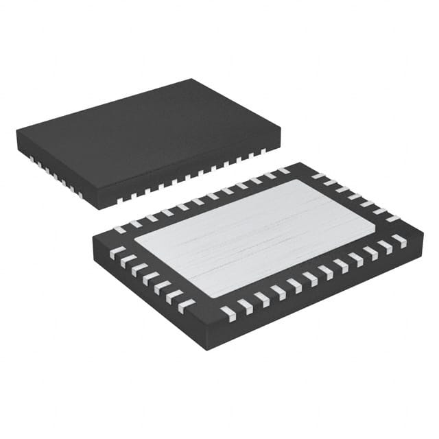
- Part No.:
- DS1875RT+
- Manufacturer:
- Analog Devices Inc./Maxim Integrated
- Category:
- Specialized
- Package:
- -
- Datasheet:
-
 DS1875RT+.pdf
- Description:
- IC SFP CTRLR/TRIPLEXER 38-TQFN
- Quantity:
- Payment:

- Shipping:

Inventory:4,289
Please send an inquiry. Send us your inquiry, and we will respond immediately.
Product details
Overview
DS1875RT+ from Maxim Integrated is a PON triplexer and SFP controller IC designed for burst-mode optical transceivers. It integrates APC loop control, temperature-indexed laser bias/modulation DACs, 10-channel ADC monitoring (including internal temperature sensor), four DAC outputs, PWM-based APD bias generation up to 90V, and full SFF-8472 diagnostics - enabling compact, compliant BPON/GPON/EPON triplexer modules.
For engineers reviewing the DS1875RT+ datasheet, DS1875RT+ pinout, DS1875RT+ application, or DS1875RT+ equivalent, this page delivers verified functional role, validated pin assignments, confirmed operating range (–40°C to +95°C), real-world diagnostic capabilities (RSSI with 29dB electrical dynamic range), and precise alternative part guidance for optical module design.
Technical Context
The DS1875RT+ implements dual closed-loop control: one APC loop using BMD input with factory-calibrated lookup tables for laser bias and modulation current vs. temperature, and a separate PWM-controlled feedback loop for APD bias with selectable switching frequencies (131.25/262.5/525/1050 kHz) and boost/buck capability. Its analog monitoring architecture supports simultaneous sampling of eight external voltage inputs (MON1–MON8), VCC, and internal die temperature with 13-bit ADC resolution and programmable full-scale ranges.
It features I²C-compatible interface (400 kHz fast-mode) with password-protected nonvolatile memory (120 bytes at main address, 128 bytes protected by second password, plus 256 bytes at A0h slave address), maskable fault shutdown via TX-F and FETG outputs, and comprehensive quick-trip alarm detection on MON3 with hysteresis configuration - all synchronized to burst-enable timing (BEN) for PON compliance.
Key Specifications
| Parameter | Value and Actual Design Meaning |
|---|---|
| Operating Voltage | +2.85V to +3.9V - powers full functionality including ADC, DACs, PWM, and I²C without external regulation |
| Temp Range | –40°C to +95°C - qualified for industrial-grade optical module operation in uncontrolled chassis environments |
| ADC Channels | 10 total: 8 external (MON1–MON8), VCC, internal temperature - enables full SFF-8472 diagnostic coverage |
| DAC Outputs | Four: DAC1 (8-bit, 2.5V range), M4DAC (8-bit, 1.25V range), two internal DACs - supports independent laser bias and modulation control |
| PWM Switching | Selectably 131.25 / 262.5 / 525 / 1050 kHz - balances efficiency, EMI, and APD response time in bias generation |
| RSSI Dynamic Range | 29dB electrical - provides accurate received signal strength indication across wide optical power variations |
| I²C Interface | 400kHz fast-mode compatible - enables real-time calibration, monitoring, and fault reporting in host-controlled SFP modules |
Pinout & Package
DS1875RT+ is housed in a 38-pin TQFN package (5mm × 7mm × 0.8mm) with exposed thermal pad (EP). The package supports high-density optical module layouts and efficient heat dissipation during APD bias generation.
| Pin/Terminal | Circuit Role | Design Meaning |
|---|---|---|
| VCC (Pins 4, 11, 24, 30) | Main supply input | Four dedicated pins reduce IR drop and improve noise immunity for analog/RF sections |
| GND (Pins 6, 7, 25, 31) | Ground reference | Multiple low-inductance ground paths isolate digital, analog, and PWM return currents |
| SW (Pin 5) | PWM switch node | Drives external inductor in boost/buck APD bias circuit; rated for up to 90V output |
| FB (Pin 27) | Feedback input | Connects to APD bias divider network; enables closed-loop regulation with error amplifier compensation |
| COMP (Pin 26) | Compensation node | Accepts RC network to stabilize PWM loop; clamped between 0.8V and 2.1V |
| BIAS (Pin 28) | Laser bias output | 8-bit DAC output controlling laser diode anode current via external transistor; supports APC loop |
| MOD (Pin 29) | Laser modulation output | 8-bit DAC output driving laser cathode modulation path; temperature-compensated via LUT |
| BEN (Pin 12) | Burst enable input | Synchronizes internal timing to PON burst window; triggers first ADC sample and APC update |
| TX-D (Pin 9) | Transmit disable | Hardware shutdown control; forces BIAS/MOD/FETG into safe state per SFF-8472 requirements |
| FETG (Pin 22) | Safety shutdown gate | Open-drain output driving external MOSFET to cut APD bias during overcurrent or fault |
| MON1–MON8 (Pins 19, 18, 17, 16, 38, 37, 36, 35) | Analog monitor inputs | Eight configurable voltage inputs supporting ±0.5V to (VCC + 0.5V); used for laser/APD/video receiver monitoring |
| SCL/SDA (Pins 34, 33) | I²C interface | Standard bidirectional bus for calibration data read/write, real-time monitoring, and fault logging |
Key Features
| Feature | Design Value |
|---|---|
| APC loop with temperature LUT | Eliminates need for external microcontroller; maintains stable laser output power across –40°C to +95°C via factory-programmed compensation curves |
| Programmable RSSI with 29dB range | Enables accurate optical power measurement in both low-light (receiver sensitivity) and high-power (burst transmission) conditions |
| Maskable fault shutdown | Allows selective disabling of laser/APD safety shutdowns (e.g., retain TX-F but suppress FETG) without compromising diagnostic integrity |
| Password-protected EEPROM | 120 bytes (PW1) + 128 bytes (PW2) + 256 bytes (A0h) - secures calibration coefficients and vendor-specific settings against unauthorized overwrite |
| Quick-trip MON3 monitoring | Dedicated high-speed comparator on MON3 with user-configurable hysteresis thresholds for critical fault detection (e.g., APD overvoltage) |
Applications
| BPON/GPON Optical Triplexer | SFP Transceiver Module |
|---|---|
Use Scenario: Integrating burst-mode laser driver, APD receiver, and video receiver in single-pluggable GPON ONU triplexer housing. IC Role / Device Role / Timing Role: DS1875RT+ serves as central controller managing APC, modulation, APD bias, and SFF-8472 diagnostics - synchronizing all functions to BEN timing. Use Value: Reduces component count by replacing discrete DACs, ADCs, and protection logic; ensures compliance with ITU-T G.984.x burst-timing requirements. | Use Scenario: Embedded in SFP+ pluggable module for fiber-to-the-home (FTTH) access networks requiring hot-plug diagnostics. IC Role / Device Role / Timing Role: DS1875RT+ acts as digital diagnostic interface (DDMI) engine, providing real-time temperature, voltage, bias, and RX power telemetry via I²C. Use Value: Enables host system to monitor link health, predict failures, and enforce eye-safety limits without external firmware intervention. |
| APD Bias Controller | Laser Safety Monitor |
Use Scenario: Generating stable, temperature-compensated high-voltage bias (up to 90V) for avalanche photodiode receivers in passive optical networks. IC Role / Device Role / Timing Role: DS1875RT+ implements closed-loop PWM control using FB/COMP pins, with optional fast shutdown via FETG output on overcurrent. Use Value: Achieves <±2%FS DAC accuracy and <±3°C thermometer error - critical for maintaining APD gain stability across temperature. | Use Scenario: Enforcing Class 1M laser safety compliance in burst-mode transmitters by monitoring bias current, modulation depth, and fault conditions. IC Role / Device Role / Timing Role: DS1875RT+ continuously samples BMD, monitors TX-D state, and asserts TX-F/FETG within 5μs of fault detection per SFF-8472. Use Value: Meets IEC 60825-1 requirements through hardware-enforced shutdown - eliminating reliance on software polling latency. |
Equivalent & Alternatives
The following parts are listed as comparable options for similar PON triplexer controller applications.
| Alternative Part | Technical Difference | Application Difference | Selection Advice |
|---|---|---|---|
| MAX3643 | Complementary laser driver IC (not controller); lacks ADC, DACs, SFF-8472 logic, and APD bias PWM - requires DS1875RT+ for full system function | Used only as laser driver stage; cannot replace DS1875RT+'s monitoring/control role | Select MAX3643 only as paired driver with DS1875RT+, not as standalone alternative |
| DS1873 | Legacy predecessor with identical pinout and core functionality but reduced ADC channels (6 vs. 10), no RSSI, lower DAC resolution (7-bit), and no A0h auxiliary memory | Suitable for cost-sensitive legacy GPON designs where full SFF-8472 compliance and enhanced diagnostics are not required | Choose DS1873 only for backward-compatible upgrades with minimal feature impact |
Compared with DS1875RT+, the DS1873 offers fewer monitoring resources and lower diagnostic fidelity, while the MAX3643 serves only as a companion driver - neither provides full functional equivalence, making DS1875RT+ the sole integrated solution for new SFP/PON triplexer designs requiring complete burst-mode control and SFF-8472 compliance.
Availability
DS1875RT+ is available at Aetrix Electronics and suitable for BPON/GPON/EPON optical triplexers, SFP/SFP+ transceiver modules, APD bias controllers, and laser safety monitoring systems requiring stable component supply, long-term lifecycle support, and RoHS-compliant packaging.
Supply support for DS1875RT+ includes scheduled delivery planning, volume procurement assistance, BOM continuity management, traceable sourcing, and lifecycle availability coordination for OEM customers, industrial embedded developers, connected-device designers, and electronics production programs.
Manufacturer
Maxim Integrated (now part of Analog Devices) is a semiconductor company specializing in precision analog, mixed-signal, and power management ICs for communications, computing, and industrial applications.
The DS1875RT+ belongs to Maxim's optical networking controller product line, engineered specifically to integrate burst-mode timing, laser/APD control, and SFF-8472 diagnostics into compact pluggable modules for passive optical networks.
FAQ
What is the primary function of the DS1875RT+ in optical transceiver modules?
The DS1875RT+ serves as a fully integrated PON triplexer and SFP controller IC. It manages laser bias and modulation via APC loops with temperature lookup tables, generates APD bias using a configurable PWM controller, monitors 10 analog signals (including internal temperature), and implements full SFF-8472 diagnostic functionality - all in a single 38-pin TQFN package. This eliminates the need for multiple discrete components in BPON/GPON/EPON modules.
Does the DS1875RT+ support both boost and buck configurations for APD bias generation?
Yes, the DS1875RT+ PWM controller supports both boost and buck modes for APD bias generation. In boost mode, it can generate up to 90V bias using optional external components (inductor, diode, capacitor). The switching frequency is selectable among 131.25kHz, 262.5kHz, 525kHz, or 1050kHz to optimize efficiency and transient response. Feedback (FB) and compensation (COMP) pins enable stable closed-loop regulation in either topology.
How does the DS1875RT+ ensure compliance with SFF-8472 diagnostic requirements?
The DS1875RT+ natively implements all mandatory SFF-8472 diagnostic functions: real-time monitoring of temperature, VCC, TX bias, TX output power, and RX input power via its 10-channel ADC and RSSI circuitry; I²C interface for host communication; and standardized memory map with alarm/warning flags. Its factory-calibrated internal temperature sensor (±3.0°C error), 29dB RSSI dynamic range, and maskable fault outputs (TX-F, FETG) meet specification requirements for digital diagnostic monitoring interfaces.
What are the memory protection features of the DS1875RT+?
The DS1875RT+ includes three tiers of password-protected nonvolatile memory: 120 bytes protected by Password-1, 128 bytes protected by Password-2 in the main device address, and 256 additional bytes located at the A0h slave address. These regions store calibration data, vendor-specific settings, and operational parameters. Access requires correct password entry via I²C, preventing unauthorized modification of critical coefficients used in APC, modulation, and RSSI calculations.
Can the DS1875RT+ operate across the full industrial temperature range without derating?
Yes, the DS1875RT+ is fully specified and tested for continuous operation from –40°C to +95°C. All key parameters - including ADC accuracy (±0.50%FS), DAC error (±1.25%FS), thermometer error (±3.0°C), supply current (5.5–10mA), and I²C timing - are guaranteed across this range. The device uses internal factory calibration and temperature-indexed LUTs to maintain performance without external compensation or firmware adjustment.
DS1875RT+ Specifications
- Product attributes
- Attribute value
- Manufacturer:
- Analog Devices Inc./Maxim Integrated
- Series:
- *
- Package/Case:
- -
- Packaging:
- Product Status:
- Obsolete
- Applications:
- -
- Interface:
- -
- Voltage - Supply:
- -
- Supplier Device Package:
- -
- Grade:
- -
- Qualification:
- -
- Mounting Type:
- -
DS1875RT+ FAQ
1.How can I place an order for DS1875RT+ through Aetrix?
Please submit a Request for Quotation (RFQ) for DS1875RT+ on Aetrix. Our sales agent will provide a competitive quotation and guide you through the order confirmation once you accept the terms.
2.Are the price and stock information for DS1875RT+ reliable?
The price and inventory of DS1875RT+ are updated periodically and may fluctuate due to market conditions. Stock and pricing data are typically refreshed every 24 hours. Quotation validity for DS1875RT+ is usually 5 days.
3.What payment methods are accepted for DS1875RT+?
We accept Wire Transfer, PayPal, Credit Card, Western Union, MoneyGram, and Escrow for DS1875RT+ transactions.
Note: Certain payment methods may incur a processing fee.
4.How is shipping managed for DS1875RT+?
DS1875RT+ orders can be shipped via leading logistics carriers, including DHL, UPS, FedEx, TNT, or Registered Mail.
Once your DS1875RT+ order is processed, you will receive an email with the shipment details and tracking number.
Note: Tracking information may take up to 24 hours to appear. Express delivery typically takes 3–5 business days.
5.How can I obtain technical support or documentation for DS1875RT+?
For technical support, including DS1875RT+ datasheets, pinout diagrams, or application guidance, please contact our engineering support team. They can provide detailed documentation and assistance for your DS1875RT+ requirements.
6.How does Aetrix verify that DS1875RT+ is sourced from the original manufacturer or authorized distributors?
All DS1875RT+ products on Aetrix are procured from qualified distributors and authorized channels. Our dedicated quality assurance team conducts strict verification, including traceability checks and, if necessary, third-party testing. This ensures that DS1875RT+ meets industry standards.
7.What is the process for return or replacement of DS1875RT+?
All DS1875RT+ units undergo pre-shipment inspection (PSI). If there is an issue with DS1875RT+, returns or replacements are accepted under the following conditions:
1.Quantity discrepancies, incorrect items, or visible external defects (such as breakage or corrosion), acknowledged by Aetrix.
2.The issue is reported within 90 days of delivery.
3.The DS1875RT+ part is unused and in its original packaging.
Return procedure for DS1875RT+:
1.Submit a request within 90 days.
2.Obtain a Return Material Authorization (RMA) from Aetrix.
DS1875RT+ Tags

-
NVT4857UKAZ
NXP Semiconductors

-
TCA8418RTWR
Texas Instruments

-
PCA9546APWR
Texas Instruments

-
MD0100N8-G
Microchip Technology

-
PCA9548APW,118
NXP Semiconductors

-
PCA9540BDP,118
NXP Semiconductors

-
PCA9548APWR
Texas Instruments

-
PCA9546APW,118
NXP Semiconductors

-
PTN3360DBS,518
NXP Semiconductors

-
PCA9546ABS,118
NXP Semiconductors

-
PCA9518PWR
Texas Instruments

-
PCA9545APW,118
NXP Semiconductors
Tech Hub

A practical engineering guide to 3.3V and 5V logic compatibility, input thresholds, resistor dividers, translator ICs, MOSFET level shifting, I2C pull-ups, timing limits and power-sequencing risks.

The 74HC595 uses push-pull logic outputs, while the TPIC6B595 uses 50 V open-drain DMOS sinks for higher-power loads. This guide compares timing, current limits, 3.3 V interfacing, load wiring, thermal…

The 74HC595 converts serial data into eight stable parallel outputs. This guide covers pin functions, shift and storage timing, OE and MR behavior, drive-current limits, cascading, voltage compatibilit…

A technical comparison of level-sensitive latches and edge-triggered flip-flops, covering timing windows, setup and hold limits, master–slave operation, time borrowing, race-through, HDL inference and…

A D latch stores one bit while Enable controls when data can pass. This reference covers gate-level operation, truth tables, transparency, setup and hold timing, LE versus OE, common ICs and practical …

An SR latch stores one bit through cross-coupled feedback. This engineering reference covers NOR and NAND implementations, truth tables, forbidden-state recovery, gated operation, switch debouncing, fa…

Latch circuits retain one bit through feedback. This technical reference covers SR and D latches, truth tables, transparency, timing limits, latch-versus-flip-flop behavior, applications and common log…

An engineering guide to LED driver operation, constant-current and constant-voltage outputs, linear and switching topologies, dimming, IC selection, calculations, replacement compatibility, and fault c…

Operational amplifier guide covering op amp basics, feedback, ideal vs real op amps, common configurations, buffer circuits, offset, bias current, gain-bandwidth, slew rate, rail-to-rail limits and sel…

Jumper cables guide covering safe connection order, red and black clamp placement, final ground connection, cable gauge, length, clamp quality, copper vs CCA cables, jump starter comparison and battery…


