
 My Inquiry
 My Account


Analog Devices Inc./Maxim Integrated DS1884AT+T
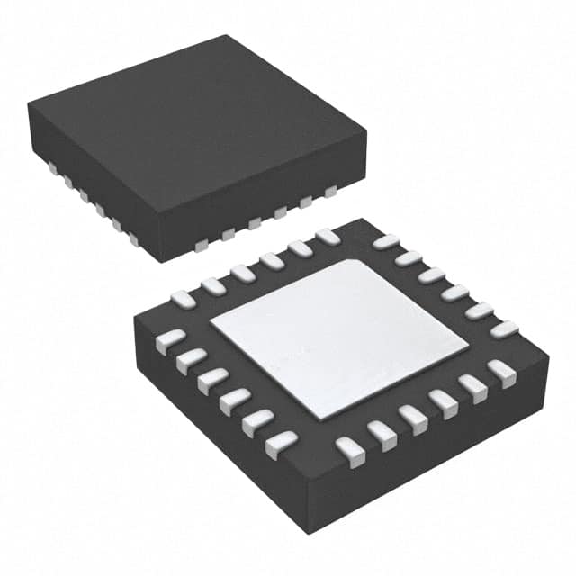
- Part No.:
- DS1884AT+T
- Manufacturer:
- Analog Devices Inc./Maxim Integrated
- Category:
- Specialized
- Package:
- 24-WFQFN Exposed Pad
- Datasheet:
-
 DS1884AT+T.pdf
- Description:
- IC INTERFACE SPECIALIZED 24TQFN
- Quantity:
- Payment:

- Shipping:

Inventory:2,227
Please send an inquiry. Send us your inquiry, and we will respond immediately.
Product details
Overview
DS1884AT+T from Maxim Integrated is a SFP and PON ONU controller with digital LDD interface, designed for optical transceiver modules compliant with SFF-8472. It provides dual closed-loop laser bias and modulation control, 13-bit ADC monitoring of VCC/temperature/laser bias/laser power/RSSI, and 9-bit temperature-compensated DAC for APD bias. It operates in GPON and 10G PON ONU systems with I²C and 3-wire master interfaces to MAX3710/MAX3945.
For engineers reviewing the DS1884AT+T datasheet, DS1884AT+T pinout, DS1884AT+T application, or DS1884AT+T equivalent, this page delivers verified functional scope, calibrated monitoring accuracy, laser control mode selection, EEPROM-based configuration storage, and fault/alarm flag architecture per SFF-8472 compliance requirements.
Technical Context
The DS1884AT+T implements a fully integrated digital control loop for laser diode drivers in pluggable optical modules, supporting three distinct laser control modes: dual closed-loop (bias + modulation), APC-only (bias auto-controlled, modulation via LUT), and open-loop (both via temperature LUTs). Its internal 13-bit ADC performs differential RSSI measurement with scalable dynamic range and supports internal calibration for laser bias, laser power, and receive power.
It integrates a 9-bit DAC with on-chip temperature compensation for APD bias control, and features flexible password protection across three security levels. Communication occurs via I²C-compatible interface and dedicated 3-wire master interface to companion laser drivers, enabling real-time register access and synchronized control of MAX3710/MAX3945 devices.
Key Specifications
| Parameter | Value and Actual Design Meaning |
|---|---|
| ADC Resolution | 13-bit - enables ±0.5°C temperature resolution and sub-mA laser bias accuracy over full industrial range. |
| DAC Resolution | 9-bit - provides 512-step APD bias control with temperature compensation for stable receiver sensitivity. |
| Laser Control Modes | Three modes: dual closed-loop, APC-only, and open-loop - selectable via register bits DPC_EN/APC_EN for system-level optimization. |
| EEPROM Capacity | 256-byte A0h + 128-byte A2h upper memory - stores calibration data, LUTs, alarm thresholds, and device configuration persistently. |
| Interface Protocols | I²C + 3-wire master - allows host MCU communication and direct register-level control of MAX3710/MAX3945 without external logic. |
| Monitoring Channels | VCC, temperature, laser bias, laser power, RSSI - all monitored with alarm/warning flags per SFF-8472 standard. |
| Security Levels | Three-tier password scheme - protects critical registers (e.g., LUTs, DAC, alarm thresholds) from unauthorized write access. |
Pinout & Package
DS1884AT+T is housed in a 24-pin TSSOP package (5.0mm × 6.5mm, 0.65mm pitch) with exposed thermal pad for enhanced thermal dissipation in high-density optical module PCB layouts.
| Pin/Terminal | Circuit Role | Design Meaning |
|---|---|---|
| VCC | Supply voltage input | 3.3V ±5% main power rail; powers internal analog/digital blocks and I/O buffers. |
| GND | Ground reference | Analog and digital ground common point; requires low-inductance connection to minimize noise coupling into ADC/DAC paths. |
| SCL | I²C clock input | Supports standard/fast-mode I²C up to 400kHz; used for host configuration and status readback. |
| SDA | I²C data bidirectional | Open-drain interface with internal pull-up; shares bus with other SFP module components (e.g., EEPROM). |
| TXD / TXDOUT | Transmit disable input/output | Active-low signal controlling laser emission; output reflects internal fault state (e.g., TXF assertion). |
| LOS / LOSOUT | Loss-of-signal input/output | Differential RSSI-derived LOS detection; output drives module LOS indicator per SFF-8472. |
| RSEL | Rate select input | Configures operating mode (e.g., GPON vs. EPON); sets internal scaling factors for RSSI and laser parameters. |
| IN1 / TXF | Status/fault monitor input | Accepts external fault signals (e.g., MAX3710 TXF) and maps them to internal alarm registers. |
| APD_BIAS | DAC output terminal | Drives APD bias voltage; value set by 9-bit DAC register with temperature compensation applied in real time. |
| TXMON | Laser monitor feedback | Accepts laser anode current sense signal for closed-loop bias control; supports internal/external calibration. |
| RSSI+ | Differential RSSI input (+) | High-side input for receive power monitoring; paired with RSSI− for common-mode rejection up to VCC. |
| RSSI− | Differential RSSI input (−) | Low-side input referenced to VCC; enables accurate optical power measurement under varying common-mode conditions. |
| CLK3W / DATA3W / CS3W | 3-wire master interface | Direct synchronous interface to MAX3710/MAX3945 for real-time laser driver register access and control. |
| NC | No-connect pins | Pins 1, 2, 3, 4, 5, 6, 7, 8, 9, 10, 11, 12, 13, 14, 15, 16, 17, 18, 19, 20, 21, 22, 23, 24 - not internally connected; must be left floating or grounded per layout guidelines. |
Key Features
| Feature | Design Value |
|---|---|
| Dual closed-loop laser control | Simultaneous automatic regulation of laser bias and modulation current using independent temperature LUTs for calibration at multiple points. |
| Differential RSSI input | Enables accurate receive power measurement across wide dynamic range while rejecting common-mode noise up to VCC level. |
| Internal direct-to-digital temperature sensor | Eliminates need for external thermistor; provides ±1°C accuracy over −40°C to +85°C for real-time LUT indexing and DAC compensation. |
| Maskable alarm/warning system | Per-channel alarm enable/disable bits allow selective monitoring (e.g., disable TXB alarm during warm-up) without firmware overhead. |
| 256-byte A0h + 128-byte A2h EEPROM | Stores vendor-specific calibration coefficients, LUTs, and user-defined configuration; retains data after power cycle. |
| Three-level password security | Prevents unauthorized writes to critical registers (e.g., MODE, DACFS, PW_ENA/B) - essential for production line programming and field updates. |
Applications
| GPON ONU Module | 10G PON ONU Module |
|---|---|
Use Scenario: Optical line termination in fiber-to-the-home networks where upstream burst-mode transmission and downstream continuous-mode reception occur. IC Role / Device Role / Timing Role: Primary controller managing laser bias/modulation, RSSI-based LOS detection, and real-time temperature compensation for burst-mode stability. Use Value: Ensures <10μs turn-on delay and <50ns jitter on burst-mode TX enable, meeting ITU-T G.984/G.987 timing specifications. | Use Scenario: Next-generation passive optical network deployment requiring higher bandwidth and improved power efficiency. IC Role / Device Role / Timing Role: Central monitoring and control unit coordinating MAX3710 laser driver and MAX3945 limiting amplifier in 10G-EPON/XGS-PON modules. Use Value: Delivers 13-bit RSSI resolution and dual-range functionality to maintain link budget margin across 20dB dynamic optical input range. |
| SFP Transceiver Module | SFP+ Transceiver Module |
Use Scenario: Pluggable 1.25Gbps optical transceivers used in enterprise switches and routers. IC Role / Device Role / Timing Role: SFF-8472-compliant digital diagnostic monitor (DDM) providing real-time VCC, temperature, TX bias, TX power, and RX power telemetry. Use Value: Enables hot-plug compatibility and host-side DDM interpretation via standardized I²C address map (A0h/A2h). | Use Scenario: High-speed 10Gbps pluggable optics deployed in data center top-of-rack switches. IC Role / Device Role / Timing Role: Digital controller interfacing with 3-wire master port to manage MAX3710 laser driver while maintaining SFF-8472 compliance for diagnostics. Use Value: Supports 10G NRZ signaling with <0.5dB power leveling error across temperature, ensuring consistent extinction ratio and eye opening. |
Equivalent & Alternatives
The following parts are listed as comparable options for similar SFP/PON controller applications.
| Alternative Part | Technical Difference | Application Difference | Selection Advice |
|---|---|---|---|
| MAX3740A | Integrated laser driver + monitor in single chip; lacks separate 3-wire master interface and APD DAC; 12-bit ADC only. | Targeted at lower-cost SFP modules without APD receivers or complex LUT-based calibration needs. | Select MAX3740A when system uses PIN photodiodes and does not require APD bias control or dual-closed-loop laser tuning. |
| DS1882 | Legacy SFP controller; no PON support, no RSEL pin, fixed APC-only mode, 12-bit ADC, no APD DAC. | Designed for basic SFF-8472 SFP modules only; incompatible with GPON/10G PON timing and control requirements. | Choose DS1882 only for cost-sensitive legacy SFP designs lacking PON features and requiring minimal feature set. |
Compared with DS1884AT+T, MAX3740A integrates laser drive but sacrifices APD bias control and PON-specific LUT flexibility, while DS1882 omits PON support entirely and offers reduced monitoring resolution-making DS1884AT+T the sole option for calibrated dual-loop GPON/10G PON ONU control.
Availability
DS1884AT+T is available at Aetrix Electronics and suitable for GPON ONU modules, 10G PON transceivers, and SFP+ optical transceivers requiring stable component supply, long-term lifecycle support, and SFF-8472 compliance assurance.
Supply support for DS1884AT+T includes scheduled delivery planning, volume procurement assistance, BOM continuity management, traceable sourcing, and lifecycle availability coordination for OEM customers, industrial embedded developers, connected-device designers, and electronics production programs.
Manufacturer
Maxim Integrated, now part of Analog Devices, designs precision analog, mixed-signal, and digital ICs for communications, computing, consumer, and industrial applications.
The DS1884AT+T belongs to Maxim's optical networking controller product line, engineered specifically for SFP, SFP+, and PON ONU modules requiring SFF-8472 compliance, dual-loop laser control, and integrated diagnostics.
FAQ
What is the primary function of the DS1884AT+T in an optical transceiver module?
The DS1884AT+T serves as the digital diagnostic monitor and laser controller in SFP, SFP+, and PON ONU modules. It implements SFF-8472-compliant monitoring of VCC, temperature, laser bias, laser power, and RSSI while providing dual closed-loop, APC-only, or open-loop laser control. The DS1884AT+T also manages communication with MAX3710/MAX3945 via its dedicated 3-wire master interface and stores calibration data in on-chip EEPROM.
Does the DS1884AT+T support both PIN and APD photodiode receivers?
Yes, the DS1884AT+T supports both receiver types. Its 9-bit DAC with temperature compensation is specifically designed for precise APD bias control, while its differential RSSI input and scalable ADC range accommodate the wider dynamic range required by APD-based systems. For PIN receivers, the same RSSI path operates with adjusted gain settings controlled by RSEL and internal register configuration.
How does the DS1884AT+T achieve temperature compensation for laser control?
The DS1884AT+T uses an internal direct-to-digital temperature sensor (±1°C accuracy) to index pre-programmed lookup tables (LUTs) for laser bias, modulation, and APC tracking error. These LUTs are stored in EEPROM and applied in real time during operation. The DS1884AT+T supports separate LUTs for BIAS, MODULATION, and SET_2XAPC, enabling multi-point calibration across the industrial temperature range.
Can the DS1884AT+T operate without external microcontroller intervention?
Yes, the DS1884AT+T can operate autonomously after initial configuration. Its internal state machine executes closed-loop control, alarm evaluation, and EEPROM-based LUT lookups without host CPU involvement. However, I²C or 3-wire master access remains available for runtime reconfiguration, fault logging, or calibration updates - making the DS1884AT+T suitable for both host-managed and standalone optical module architectures.
What memory resources are available on the DS1884AT+T for storing calibration data?
The DS1884AT+T provides 256 bytes of A0h memory and 128 bytes of A2h upper memory for nonvolatile storage. This includes space for temperature LUTs (BIAS, MODULATION, APC), calibration offsets/scales for ADC channels (VCC, TXB, TXP, RSSI), alarm/warning thresholds, device identification, and password entries. All memory is accessible via standard SFF-8472 I²C addressing and supports byte-write and page-write operations.
DS1884AT+T Specifications
- Product attributes
- Attribute value
- Manufacturer:
- Analog Devices Inc./Maxim Integrated
- Series:
- -
- Package/Case:
- 24-WFQFN Exposed Pad
- Packaging:
- Tape & Reel (TR)
- Product Status:
- Obsolete
- Applications:
- -
- Interface:
- I2C
- Voltage - Supply:
- 2.85V ~ 3.6V
- Supplier Device Package:
- 24-TQFN (4x5)
- Grade:
- -
- Qualification:
- -
- Mounting Type:
- Surface Mount
DS1884AT+T FAQ
1.How can I place an order for DS1884AT+T through Aetrix?
Please submit a Request for Quotation (RFQ) for DS1884AT+T on Aetrix. Our sales agent will provide a competitive quotation and guide you through the order confirmation once you accept the terms.
2.Are the price and stock information for DS1884AT+T reliable?
The price and inventory of DS1884AT+T are updated periodically and may fluctuate due to market conditions. Stock and pricing data are typically refreshed every 24 hours. Quotation validity for DS1884AT+T is usually 5 days.
3.What payment methods are accepted for DS1884AT+T?
We accept Wire Transfer, PayPal, Credit Card, Western Union, MoneyGram, and Escrow for DS1884AT+T transactions.
Note: Certain payment methods may incur a processing fee.
4.How is shipping managed for DS1884AT+T?
DS1884AT+T orders can be shipped via leading logistics carriers, including DHL, UPS, FedEx, TNT, or Registered Mail.
Once your DS1884AT+T order is processed, you will receive an email with the shipment details and tracking number.
Note: Tracking information may take up to 24 hours to appear. Express delivery typically takes 3–5 business days.
5.How can I obtain technical support or documentation for DS1884AT+T?
For technical support, including DS1884AT+T datasheets, pinout diagrams, or application guidance, please contact our engineering support team. They can provide detailed documentation and assistance for your DS1884AT+T requirements.
6.How does Aetrix verify that DS1884AT+T is sourced from the original manufacturer or authorized distributors?
All DS1884AT+T products on Aetrix are procured from qualified distributors and authorized channels. Our dedicated quality assurance team conducts strict verification, including traceability checks and, if necessary, third-party testing. This ensures that DS1884AT+T meets industry standards.
7.What is the process for return or replacement of DS1884AT+T?
All DS1884AT+T units undergo pre-shipment inspection (PSI). If there is an issue with DS1884AT+T, returns or replacements are accepted under the following conditions:
1.Quantity discrepancies, incorrect items, or visible external defects (such as breakage or corrosion), acknowledged by Aetrix.
2.The issue is reported within 90 days of delivery.
3.The DS1884AT+T part is unused and in its original packaging.
Return procedure for DS1884AT+T:
1.Submit a request within 90 days.
2.Obtain a Return Material Authorization (RMA) from Aetrix.
DS1884AT+T Tags

-
NVT4857UKAZ
NXP Semiconductors

-
TCA8418RTWR
Texas Instruments

-
PCA9546APWR
Texas Instruments

-
MD0100N8-G
Microchip Technology

-
PCA9548APW,118
NXP Semiconductors

-
PCA9540BDP,118
NXP Semiconductors

-
PCA9548APWR
Texas Instruments

-
PCA9546APW,118
NXP Semiconductors

-
PTN3360DBS,518
NXP Semiconductors

-
PCA9546ABS,118
NXP Semiconductors

-
PCA9518PWR
Texas Instruments

-
PCA9545APW,118
NXP Semiconductors
Tech Hub

A practical engineering guide to 3.3V and 5V logic compatibility, input thresholds, resistor dividers, translator ICs, MOSFET level shifting, I2C pull-ups, timing limits and power-sequencing risks.

The 74HC595 uses push-pull logic outputs, while the TPIC6B595 uses 50 V open-drain DMOS sinks for higher-power loads. This guide compares timing, current limits, 3.3 V interfacing, load wiring, thermal…

The 74HC595 converts serial data into eight stable parallel outputs. This guide covers pin functions, shift and storage timing, OE and MR behavior, drive-current limits, cascading, voltage compatibilit…

A technical comparison of level-sensitive latches and edge-triggered flip-flops, covering timing windows, setup and hold limits, master–slave operation, time borrowing, race-through, HDL inference and…

A D latch stores one bit while Enable controls when data can pass. This reference covers gate-level operation, truth tables, transparency, setup and hold timing, LE versus OE, common ICs and practical …

An SR latch stores one bit through cross-coupled feedback. This engineering reference covers NOR and NAND implementations, truth tables, forbidden-state recovery, gated operation, switch debouncing, fa…

Latch circuits retain one bit through feedback. This technical reference covers SR and D latches, truth tables, transparency, timing limits, latch-versus-flip-flop behavior, applications and common log…

An engineering guide to LED driver operation, constant-current and constant-voltage outputs, linear and switching topologies, dimming, IC selection, calculations, replacement compatibility, and fault c…

Operational amplifier guide covering op amp basics, feedback, ideal vs real op amps, common configurations, buffer circuits, offset, bias current, gain-bandwidth, slew rate, rail-to-rail limits and sel…

Jumper cables guide covering safe connection order, red and black clamp placement, final ground connection, cable gauge, length, clamp quality, copper vs CCA cables, jump starter comparison and battery…


