
 My Inquiry
 My Account


Analog Devices Inc./Maxim Integrated DS1884T+T
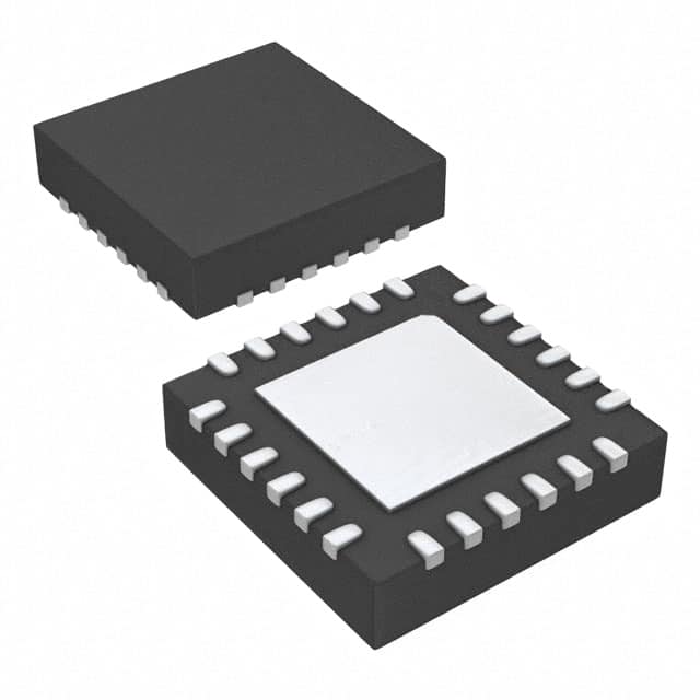
- Part No.:
- DS1884T+T
- Manufacturer:
- Analog Devices Inc./Maxim Integrated
- Category:
- Specialized
- Package:
- 24-WFQFN Exposed Pad
- Datasheet:
-
 DS1884T+T.pdf
- Description:
- IC INTERFACE SPECIALIZED 24TQFN
- Quantity:
- Payment:

- Shipping:

Inventory:3,979
Please send an inquiry. Send us your inquiry, and we will respond immediately.
Product details
Overview
DS1884T+T from Maxim Integrated is a SFP and PON ONU controller with digital LDD interface, designed for real-time laser bias and modulation control, APC set-point tracking, and comprehensive monitoring of VCC, temperature, laser bias current, laser output power, and differential RSSI. It integrates a 13-bit ADC and 9-bit DAC with temperature compensation, supporting GPON and 10G PON ONU modules up to 2.5GHz.
For engineers reviewing the DS1884T+T datasheet, DS1884T+T pinout, DS1884T+T application, or DS1884T+T equivalent, this device serves as a companion controller to MAX3710/MAX3945 transceiver ICs in SFF-8472-compliant optical modules-requiring precise dual-closed-loop calibration, alarm/warning flag management, and I²C/3-wire master interface coordination.
Technical Context
The DS1884T+T implements three configurable laser control modes: dual closed-loop (bias + modulation auto-controlled via dual LUTs), APC-only loop (bias auto-controlled, modulation driven by temperature LUT), and open-loop (both bias and modulation driven by independent temperature LUTs). Its 13-bit ADC supports internal/external calibration for laser bias, laser power, and differential receive power, with scalable dynamic range and alarm/warning flags per channel.
A dedicated 9-bit DAC provides temperature-compensated APD bias control. The device communicates via I²C-compatible interface and a 3-wire master interface to drive the MAX3710 laser driver/limiting amplifier, enabling synchronized transmitter/receiver functionality in SFP+ and PON ONU applications.
Key Specifications
| Parameter | Value and Actual Design Meaning |
|---|---|
| ADC Resolution | 13-bit, enabling high-precision monitoring of VCC, temperature, laser bias, laser power, and RSSI with internal calibration support |
| DAC Resolution | 9-bit with temperature compensation, used for accurate APD bias voltage control across operating temperature range |
| Laser Control Modes | Three modes: dual closed-loop, APC-only, and open-loop-each configurable via register settings and LUT indexing |
| RSSI Input | Differential input with dual-range functionality, supporting common-mode to VCC and enhanced LOS detection accuracy |
| Interface Protocols | I²C-compatible slave interface + dedicated 3-wire master interface for direct communication with MAX3710/MAX3945 |
| Memory | 256-byte A0h EEPROM + 128-byte upper A2h EEPROM for configuration storage, password protection, and calibration data |
| Security | Flexible three-level password scheme (PW1/PW2) for access control to critical registers and memory regions |
Pinout & Package
DS1884T+T is housed in a 24-pin TSSOP package (5.0mm × 7.8mm, 0.65mm pitch) with exposed thermal pad for improved thermal performance in optical module environments.
| Pin/Terminal | Circuit Role | Design Meaning |
|---|---|---|
| VCC | Power supply input | 3.3V nominal supply; powers internal analog/digital circuitry and supports low-voltage operation down to 3.0V |
| GND | Ground reference | Analog and digital ground shared; requires low-impedance connection for ADC/DAC accuracy |
| SCL | I²C clock input | Supports standard/fast-mode I²C up to 400kHz for host communication and memory access |
| SDA | I²C data I/O | Open-drain bidirectional line for configuration, monitoring, and EEPROM read/write operations |
| TXD / TXDOUT | Transmit disable input/output | Active-low signal controlling laser enable/disable; bidirectional for status feedback to host |
| LOS / LOSOUT | Loss-of-signal input/output | Differential RSSI-derived LOS detection with maskable alarm flag and output assertion |
| RSEL | Rate select input | Configures data rate mode (e.g., GPON vs. 10G PON) for appropriate LUT selection and timing behavior |
| IN1 / TXF | Status monitor / transmit fault input | Monitors external fault conditions (e.g., MAX3710 FAULT pin); triggers alarm if asserted |
| TXMON | Laser bias/power monitor output | Analog output proportional to laser bias current or modulation current for external validation |
| APD_BIAS | APD bias DAC output | Temperature-compensated analog voltage output driving APD cathode in PIN/APD mode |
| RSSI+ | Differential RSSI input positive | High-side input for receive power measurement; supports common-mode voltage up to VCC |
| RSSI− | Differential RSSI input negative | Low-side input completing differential pair; enables noise-immune optical power monitoring |
| TEMP | Internal temperature sensor output | Direct-to-digital temperature reading via on-die sensor; used for LUT indexing and compensation |
| REFIN | ADC reference input | Accepts external reference for improved ADC accuracy or defaults to internal 2.048V reference |
Key Features
| Feature | Design Value |
|---|---|
| SFF-8472 compliance | Fully implements all required control and monitoring functions for SFP/SFP+/XFP modules, including DOM registers and alarm/warning thresholds |
| Dual closed-loop calibration | Uses separate BIAS and MODULATION LUTs to correct tracking error across temperature, enabling stable optical output over −5°C to +85°C |
| Enhanced RSSI monitoring | Differential input with coarse/fine scaling and dual-range functionality improves LOS detection resolution at low and high receive power levels |
| 3-wire master interface | Dedicated serial interface for real-time register access and control of MAX3710 laser driver without host CPU intervention |
| Password-protected memory | Three-tier security (PW1/PW2/PW_EN) prevents unauthorized access to calibration data, LUTs, and critical configuration registers |
Applications
| GPON ONU Module | 10G PON ONU Module |
|---|---|
Use Scenario: Optical line terminal (OLT) to customer premises equipment (CPE) downstream transmission in fiber-to-the-home networks. IC Role / Device Role / Timing Role: Primary controller managing laser bias, modulation, APC tracking, and RSSI-based LOS detection in GPON burst-mode operation. Use Value: Enables compliant SFF-8472 DOM reporting, temperature-compensated power leveling, and fast LOS recovery within GPON's 125μs guard time. | Use Scenario: High-bandwidth upstream/downstream data transmission in next-generation passive optical networks. IC Role / Device Role / Timing Role: Dual-mode controller supporting both GPON and XG-PON rates via RSEL configuration and optimized LUT sets. Use Value: Maintains <±0.5dB optical power stability across temperature using dual-closed-loop calibration, meeting XG-PON Class B/C power specifications. |
| SFP+ Transceiver Module | Industrial Optical Data Link |
Use Scenario: 10G Ethernet interconnect in enterprise switches, routers, and base stations. IC Role / Device Role / Timing Role: Companion controller to MAX3710, providing laser control, monitoring, and I²C-based DOM interface for host system telemetry. Use Value: Delivers full SFF-8472 compliance including real-time TX_PWR, RX_PWR, TEMP, VCC, and TX_BIAS reporting with alarm/warning flags. | Use Scenario: Harsh-environment fiber links in industrial automation, smart grid, or transportation systems. IC Role / Device Role / Timing Role: Robust optical controller with extended temperature operation, fault masking, and traceable calibration data storage. Use Value: Ensures reliable LOS detection and laser safety shutdown under voltage fluctuation or thermal stress via programmable alarm thresholds and password-locked configuration. |
Equivalent & Alternatives
The following parts are listed as comparable options for similar SFP/PON optical controller applications.
| Alternative Part | Technical Difference | Application Difference | Selection Advice |
|---|---|---|---|
| MAX3740A | Integrated laser driver + monitor in single chip; lacks dedicated 3-wire master interface and dual-LUT APC architecture | Targeted at lower-cost SFP modules without advanced power leveling or PON burst-mode requirements | Choose MAX3740A when system integration priority outweighs fine-grained APC tracking and LUT flexibility |
| DS1878 | Successor device with enhanced 16-bit ADC, faster I²C, and expanded memory; pin-compatible but requires firmware update | Designed for next-gen 25G/50G PON and coherent SFP modules requiring higher resolution monitoring | Choose DS1878 for new designs targeting extended bandwidth, tighter optical tolerance, or future-proofing |
Compared with MAX3740A, DS1884T+T delivers superior APC tracking accuracy via dual-LUT compensation and dedicated 3-wire control-critical for PON burst-mode stability. Against DS1878, DS1884T+T offers proven qualification in GPON/10G PON deployments with mature firmware ecosystems and lower cost-of-ownership in volume production.
Availability
DS1884T+T is available at Aetrix Electronics and suitable for GPON ONU modules, 10G PON transceivers, and SFP+ optical interconnects requiring stable component supply, long-term lifecycle support, and SFF-8472 compliance.
Supply support for DS1884T+T includes scheduled delivery planning, volume procurement assistance, BOM continuity management, traceable sourcing, and lifecycle availability coordination for OEM customers, industrial embedded developers, connected-device designers, and electronics production programs.
Manufacturer
Maxim Integrated, now part of Analog Devices, designs precision analog, mixed-signal, and power management ICs for communications, computing, and industrial applications.
The DS1884T+T belongs to Maxim's optical networking controller product line, engineered specifically for SFF-compliant pluggable modules requiring integrated laser control, real-time monitoring, and robust digital interface coordination with laser drivers and limiting amplifiers.
FAQ
What is the primary function of the DS1884T+T in an SFP module?
The DS1884T+T serves as the core digital controller for SFP/SFP+ modules, implementing SFF-8472-compliant monitoring (temperature, VCC, TX bias, TX power, RX power) and laser control (APC, DPC, open-loop modes). It coordinates with external laser drivers like the MAX3710 via its dedicated 3-wire master interface and provides I²C access for host system telemetry-making DS1884T+T essential for DOM functionality and optical stability in commercial and PON applications.
Does the DS1884T+T support both PIN and APD photodiode configurations?
Yes, the DS1884T+T supports both PIN and APD receiver configurations through its programmable APD bias DAC output (APD_BIAS pin) and differential RSSI input stage. In APD mode, the 9-bit DAC delivers temperature-compensated bias voltage; in PIN mode, the same RSSI path operates with adjusted gain and offset scaling-configurable via A2h Table 02h registers such as RSSI_COARSE_SCALE and RSSI_FINE_OFFSET. This dual-mode capability is explicitly validated in the DS1884T+T datasheet's "APD Mode" and "PIN Mode" sections.
How does the DS1884T+T achieve APC tracking error compensation?
The DS1884T+T achieves APC tracking error compensation using a temperature lookup table (LUT) architecture with separate BIAS and MODULATION LUTs. Each LUT contains pre-programmed values indexed by internal die temperature (measured by the on-chip 13-bit ADC thermometer), allowing real-time correction of laser bias and modulation currents across −5°C to +85°C. This dual-LUT method-documented in DS1884T+T's "Temperature Lookup Table (LUT)" feature and "Dual Closed-Loop Mode" description-enables sub-0.5dB optical power variation in GPON burst-mode operation.
Can the DS1884T+T operate independently without a companion laser driver?
No, the DS1884T+T is not a standalone laser driver; it is a controller IC that requires external laser driver ICs such as the MAX3710 or MAX3945 to generate bias and modulation currents. Its TXMON pin provides analog monitoring outputs, but it lacks high-current output stages. The DS1884T+T's 3-wire master interface is specifically designed to configure and command those drivers-confirming its role as a supervisory controller rather than a power device. All functional block diagrams and typical operating circuits in the DS1884T+T datasheet show co-location with MAX3710/MAX3945.
What security features does the DS1884T+T provide for optical module firmware?
The DS1884T+T implements a three-level password protection scheme using two 32-bit passwords (PW1 and PW2) stored in A2h Table 02h registers B0h–BFh and B4h–B7h, controlled by PW_ENA and PW_ENB bits. This allows selective locking of memory pages (A0h/A2h), critical registers (e.g., MODE, TBLSEL), and calibration LUTs-preventing unauthorized modification during manufacturing or field operation. Password entry is performed via the PWE register (7Bh–7Eh), and access attempts trigger audit flags in STATUS register (6Eh), ensuring DS1884T+T meets optical module security requirements for Tier-1 network equipment.
DS1884T+T Specifications
- Product attributes
- Attribute value
- Manufacturer:
- Analog Devices Inc./Maxim Integrated
- Series:
- -
- Package/Case:
- 24-WFQFN Exposed Pad
- Packaging:
- Tape & Reel (TR)
- Product Status:
- Obsolete
- Applications:
- -
- Interface:
- I2C
- Voltage - Supply:
- 2.85V ~ 3.6V
- Supplier Device Package:
- 24-TQFN (4x5)
- Grade:
- -
- Qualification:
- -
- Mounting Type:
- Surface Mount
DS1884T+T FAQ
1.How can I place an order for DS1884T+T through Aetrix?
Please submit a Request for Quotation (RFQ) for DS1884T+T on Aetrix. Our sales agent will provide a competitive quotation and guide you through the order confirmation once you accept the terms.
2.Are the price and stock information for DS1884T+T reliable?
The price and inventory of DS1884T+T are updated periodically and may fluctuate due to market conditions. Stock and pricing data are typically refreshed every 24 hours. Quotation validity for DS1884T+T is usually 5 days.
3.What payment methods are accepted for DS1884T+T?
We accept Wire Transfer, PayPal, Credit Card, Western Union, MoneyGram, and Escrow for DS1884T+T transactions.
Note: Certain payment methods may incur a processing fee.
4.How is shipping managed for DS1884T+T?
DS1884T+T orders can be shipped via leading logistics carriers, including DHL, UPS, FedEx, TNT, or Registered Mail.
Once your DS1884T+T order is processed, you will receive an email with the shipment details and tracking number.
Note: Tracking information may take up to 24 hours to appear. Express delivery typically takes 3–5 business days.
5.How can I obtain technical support or documentation for DS1884T+T?
For technical support, including DS1884T+T datasheets, pinout diagrams, or application guidance, please contact our engineering support team. They can provide detailed documentation and assistance for your DS1884T+T requirements.
6.How does Aetrix verify that DS1884T+T is sourced from the original manufacturer or authorized distributors?
All DS1884T+T products on Aetrix are procured from qualified distributors and authorized channels. Our dedicated quality assurance team conducts strict verification, including traceability checks and, if necessary, third-party testing. This ensures that DS1884T+T meets industry standards.
7.What is the process for return or replacement of DS1884T+T?
All DS1884T+T units undergo pre-shipment inspection (PSI). If there is an issue with DS1884T+T, returns or replacements are accepted under the following conditions:
1.Quantity discrepancies, incorrect items, or visible external defects (such as breakage or corrosion), acknowledged by Aetrix.
2.The issue is reported within 90 days of delivery.
3.The DS1884T+T part is unused and in its original packaging.
Return procedure for DS1884T+T:
1.Submit a request within 90 days.
2.Obtain a Return Material Authorization (RMA) from Aetrix.
DS1884T+T Tags

-
NVT4857UKAZ
NXP Semiconductors

-
TCA8418RTWR
Texas Instruments

-
PCA9546APWR
Texas Instruments

-
MD0100N8-G
Microchip Technology

-
PCA9548APW,118
NXP Semiconductors

-
PCA9540BDP,118
NXP Semiconductors

-
PCA9548APWR
Texas Instruments

-
PCA9546APW,118
NXP Semiconductors

-
PTN3360DBS,518
NXP Semiconductors

-
PCA9546ABS,118
NXP Semiconductors

-
PCA9518PWR
Texas Instruments

-
PCA9545APW,118
NXP Semiconductors
Tech Hub

A practical engineering guide to 3.3V and 5V logic compatibility, input thresholds, resistor dividers, translator ICs, MOSFET level shifting, I2C pull-ups, timing limits and power-sequencing risks.

The 74HC595 uses push-pull logic outputs, while the TPIC6B595 uses 50 V open-drain DMOS sinks for higher-power loads. This guide compares timing, current limits, 3.3 V interfacing, load wiring, thermal…

The 74HC595 converts serial data into eight stable parallel outputs. This guide covers pin functions, shift and storage timing, OE and MR behavior, drive-current limits, cascading, voltage compatibilit…

A technical comparison of level-sensitive latches and edge-triggered flip-flops, covering timing windows, setup and hold limits, master–slave operation, time borrowing, race-through, HDL inference and…

A D latch stores one bit while Enable controls when data can pass. This reference covers gate-level operation, truth tables, transparency, setup and hold timing, LE versus OE, common ICs and practical …

An SR latch stores one bit through cross-coupled feedback. This engineering reference covers NOR and NAND implementations, truth tables, forbidden-state recovery, gated operation, switch debouncing, fa…

Latch circuits retain one bit through feedback. This technical reference covers SR and D latches, truth tables, transparency, timing limits, latch-versus-flip-flop behavior, applications and common log…

An engineering guide to LED driver operation, constant-current and constant-voltage outputs, linear and switching topologies, dimming, IC selection, calculations, replacement compatibility, and fault c…

Operational amplifier guide covering op amp basics, feedback, ideal vs real op amps, common configurations, buffer circuits, offset, bias current, gain-bandwidth, slew rate, rail-to-rail limits and sel…

Jumper cables guide covering safe connection order, red and black clamp placement, final ground connection, cable gauge, length, clamp quality, copper vs CCA cables, jump starter comparison and battery…


