
 My Inquiry
 My Account


Analog Devices Inc./Maxim Integrated DS2045AB-70#
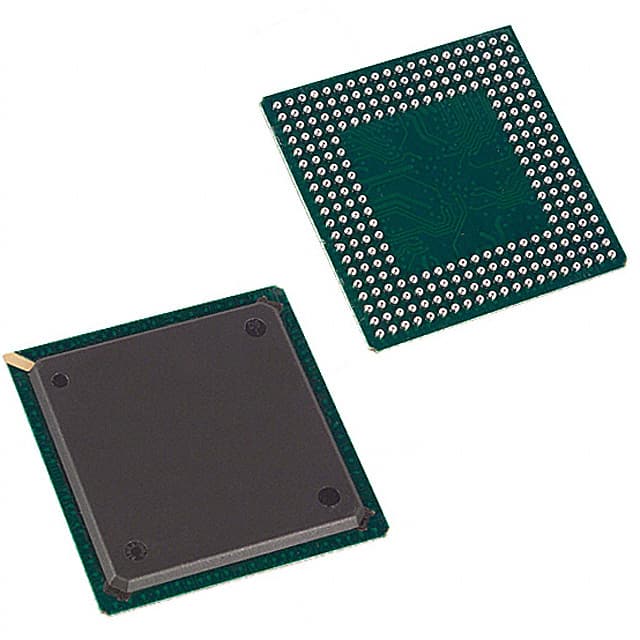
- Part No.:
- DS2045AB-70#
- Manufacturer:
- Analog Devices Inc./Maxim Integrated
- Category:
- Memory
- Package:
- 256-BGA
- Datasheet:
-
 DS2045AB-70#.pdf
- Description:
- IC NVSRAM 1MBIT PARALLEL 256BGA
- Quantity:
- Payment:

- Shipping:

Inventory:192
Please send an inquiry. Send us your inquiry, and we will respond immediately.
Product details
Overview
DS2045AB-70# from Maxim Integrated is a 1Mb (128k × 8) reflowable nonvolatile SRAM integrating static RAM, NV controller, and rechargeable manganese lithium (ML) battery in a single 256-ball 27mm² BGA module. It provides unconditional write protection at VCC < 4.75V, automatic battery switchover during power failure, and open-drain RST output for microprocessor supervision - deployed in RAID systems, industrial controllers, and fire alarm backup memory.
For engineers reviewing the DS2045AB-70# datasheet, DS2045AB-70# pinout, DS2045AB-70# application, or DS2045AB-70# equivalent, key selection considerations include 70ns access time, 5% VCC tolerance trip point, industrial temperature range (–40°C to +85°C), battery-backed data retention up to 3 years per charge, and compatibility with standard BGA reflow assembly.
Technical Context
The DS2045AB-70# implements autonomous power-fail detection using an internal voltage reference (VTP = 4.50V min) and redundant logic to unconditionally disable writes and isolate SRAM when VCC drops below tolerance. Its NV controller manages seamless transition between VCC and ML battery supply without external circuitry, maintaining data integrity during brownouts.
It features a dedicated open-drain RST output with 10mA sink capability, timed reset assertion (tRPD ≤ 3.0µs) and deassertion (tRPU = 225–525ms), synchronized to VCC recovery and tREC (125ms) to ensure SRAM readiness before CPU access.
Key Specifications
| Parameter | Value and Actual Design Meaning |
|---|---|
| Memory Size | 1Mb (128k × 8 bits) - supports full byte-wide data bus interfacing with 17 address lines (A0–A16). |
| Access Time | 70ns - enables direct replacement of standard 70ns SRAM in legacy 8051/8086-based systems without timing redesign. |
| VCC Tolerance | ±5% (4.75V–5.25V) - triggers write protection at 4.50V min, ensuring data integrity during gradual rail collapse. |
| Data Retention | Up to 3 years per full charge - achieved via internal ML battery with no external capacitor or supercap required. |
| Operating Temp | –40°C to +85°C - validated across full industrial range with guaranteed tDR, tRC, and VTP stability. |
| RST Output | Open-drain, 10mA sink - requires external pullup (1kΩ–10kΩ); used as CPU supervisor with programmable timeout coordination. |
| Package | 256-ball PBGA, 27mm² footprint - RoHS-compliant, reflow-solderable, UL Recognized (E99151). |
Pinout & Package
DS2045AB-70# uses a 256-ball plastic ball grid array (PBGA) package measuring 27mm², designed for standard convection reflow assembly (peak 225°C). All balls are arranged in a 20×20 array with corner balls omitted; ground and no-connect balls provide mechanical stability and EMI shielding.
| Pin/Terminal | Circuit Role | Design Meaning |
|---|---|---|
| A1–A4, V1–V4, W1–W4, Y1–Y4, A17–A20, W17–W20, Y17–Y20 | GND | Multiple distributed ground connections reduce noise coupling and improve power integrity during high-speed read/write cycles. |
| B1–B4, C17–C20, A5–A16, U5–U16, V5–V16, W5–W16, Y5–Y16 | N.C. | No-connect balls - reserved for mechanical reinforcement and thermal dissipation; must remain unconnected on PCB. |
| C1–C4, D1–D4, D17–D20, E17–E20, F17–F20, G17–G20, H17–H20, J17–J20, K17–K20, L17–L20, M17–M20, N17–N20, P17–P20, R17–R20, T17–T20, U17–U20, V17–V20 | A0–A16 | 17-bit address bus - supports full 128k-word addressing; all inputs TTL-compatible with VIH ≥ 2.2V, VIL ≤ 0.8V. |
| E1–E4 | RST | Open-drain reset output - asserts low during VCC undervoltage; requires external pullup for logic-high level and CPU reset coordination. |
| F1–F4 | VCC | Main 5V supply input - powers SRAM, NV controller, and charges ML battery; monitored continuously for trip-point detection. |
| G1–G4 | WE | Write enable input - active-low; controls write strobe timing; tWP = 55–75ns ensures reliable data capture with CE synchronization. |
| H1–H4 | OE | Output enable input - active-low; enables DQ0–DQ7 drivers during read; high during write to prevent bus contention. |
| J1–J4 | CE | Chip enable input - active-low; gates all internal operations; tPD = 1.5µs ensures rapid write-protection activation on power loss. |
| K1–K4 to U1–U4 | DQ0–DQ7 | 8-bit bidirectional data bus - CMOS-compatible I/O with IOL = 2.0mA, IOH = –1.0mA; high-impedance when CE or OE inactive. |
Key Features
| Feature | Design Value |
|---|---|
| Single-piece reflowable BGA | Eliminates manual battery insertion and post-soldering handling - compatible with automated SMT lines and IPC/JEDEC J-STD-020 profiles. |
| Internal ML battery + charger | UL-recognized charging circuit with short-circuit protection and temperature-stabilized reference - achieves full charge in ≤96 hours at VCC > VTP. |
| Unconditional write protection | Hardware-enforced lockout at VCC < 4.50V - no software dependency or external watchdog required to prevent corruption during brownout. |
| Automatic battery switchover | Seamless transition at VSW ≈ 2.7V - maintains SRAM power without glitch or hold-time violation, preserving state across power interruptions. |
| Reset output for CPU supervision | RST timing coordinated with tREC (125ms) and tRPU (225–525ms) - guarantees SRAM readiness before processor resumes execution. |
Applications
| RAID Systems & Servers | Industrial Controllers |
|---|---|
Use Scenario: Persistent caching of configuration metadata and journal logs during unexpected AC loss or PSU failure. IC Role / Device Role / Timing Role: Nonvolatile SRAM providing immediate-access, battery-backed storage with 70ns read/write latency and no wear-out mechanism. Use Value: Eliminates need for EEPROM/flash write endurance management and avoids 10ms+ flash programming delays during power-down sequences. | Use Scenario: Retaining PLC ladder logic state, I/O mapping, and calibration coefficients during factory line power cycling or brownouts. IC Role / Device Role / Timing Role: Direct-memory-mapped NV SRAM interfaced to 8051 or ARM Cortex-M3 via parallel bus with CE/OE/WE control. Use Value: Guarantees sub-millisecond data retention activation (tPD ≤ 1.5µs) and eliminates external backup capacitors or supervisory ICs. |
| Fire Alarm Panels | Data-Acquisition Systems |
Use Scenario: Storing alarm event timestamps, sensor fault history, and evacuation logs across extended mains outages. IC Role / Device Role / Timing Role: UL-recognized, battery-integrated memory module operating continuously at –40°C to +85°C with 3-year retention per charge. Use Value: Meets EN54-4 compliance for uninterrupted operation without periodic battery replacement or maintenance intervention. | Use Scenario: Capturing high-speed analog waveform snapshots in oscilloscopes or power quality analyzers during transient grid events. IC Role / Device Role / Timing Role: High-bandwidth (≥14MHz random access) SRAM buffer with deterministic 70ns access and automatic fail-safe write-lock. Use Value: Enables gap-free acquisition at full sampling rate even during brief (<100ms) utility sags, with zero firmware overhead. |
Equivalent & Alternatives
The following parts are listed as comparable options for similar nonvolatile SRAM applications.
| Alternative Part | Technical Difference | Application Difference | Selection Advice |
|---|---|---|---|
| DS1245Y-120+ | Legacy 28-pin DIP; no integrated battery - requires external lithium battery and discrete charger/controller; 120ns access. | Suitable only for through-hole designs with space for external support components; not reflow-compatible. | Select DS1245Y-120+ only for legacy board refresh where DIP footprint and manual battery integration are acceptable. |
| FM24CL16B | 128Kb F-RAM; I²C interface; 3.3V operation; no battery or power-fail circuitry - intrinsic nonvolatility via ferroelectric core. | Requires serial interface redesign; lower density (128Kb vs 1Mb); unsuitable for parallel-bus systems or high-throughput logging. | Choose FM24CL16B for ultra-low-power, high-endurance (10¹⁴ cycles) logging where parallel bus and 1Mb capacity are not required. |
Compared with DS1245Y-120+, DS2045AB-70# delivers 14× higher density, eliminates external battery management, and supports modern SMT assembly - while FM24CL16B trades parallel interface and capacity for infinite write endurance and simpler power architecture, but cannot replace DS2045AB-70# in byte-wide, high-speed, battery-backed applications.
Availability
DS2045AB-70# is available at Aetrix Electronics and suitable for RAID systems, industrial controllers, and fire alarm panels requiring stable component supply, long-term data retention, and RoHS-compliant BGA packaging.
Supply support for DS2045AB-70# includes scheduled delivery planning, volume procurement assistance, BOM continuity management, traceable sourcing, and lifecycle availability coordination for OEM customers, industrial embedded developers, connected-device designers, and electronics production programs.
Manufacturer
Maxim Integrated (now part of Analog Devices) is a semiconductor company specializing in precision analog, mixed-signal, and power management ICs for industrial, computing, and communications markets.
The DS2045AB-70# belongs to Maxim's nonvolatile memory product line, engineered to replace battery-backed SRAM modules with integrated power-fail protection and reflowable packaging for mission-critical data retention in harsh environments.
FAQ
What is the guaranteed data retention time for DS2045AB-70# under normal operating conditions?
The DS2045AB-70# provides up to 3 years of data retention per full battery charge at +25°C, based on component selection, process control, and design validation. This assumes initial 96-hour charge at VCC > VTP and no more than two 230°C reflow exposures. Retention is specified under data sheet Note 8 and does not require external capacitors or circuitry.
Does DS2045AB-70# require external components for battery charging or reset functionality?
No, DS2045AB-70# integrates all necessary battery charging circuitry, including UL-recognized short-circuit protection and temperature-stabilized voltage reference. The RST output is open-drain and requires only an external pullup resistor (1kΩ–10kΩ); no additional supervisor ICs, capacitors, or diodes are needed for basic operation.
How does DS2045AB-70# differ from DS2045Y-70# in terms of power monitoring?
DS2045AB-70# uses a 5% VCC tolerance threshold (VTP = 4.50V min at VCC = 5.0V), triggering write protection earlier than DS2045Y-70#, which uses a 10% threshold (VTP = 4.25V min). This makes DS2045AB-70# more sensitive to marginal supply conditions - ideal for systems requiring tighter voltage margin control.
Can DS2045AB-70# be used as a drop-in replacement for standard 70ns SRAMs like AS6C8008 or IS61LV5128?
Yes, DS2045AB-70# is pin-compatible and functionally compatible with 70ns 128k × 8 parallel SRAMs in 256-ball BGA packages. Its CE/OE/WE timing and DC/AC specifications meet or exceed JEDEC standards for 5V SRAMs, enabling direct substitution where nonvolatility and battery backup are added requirements.
What is the maximum recommended soldering temperature profile for DS2045AB-70#?
DS2045AB-70# follows IPC/JEDEC J-STD-020: peak reflow temperature is 225°C +0/–5°C, held for 10–30 seconds within ±5°C of peak; ramp-up rate ≤3°C/sec; preheat 100–150°C for 60–120 sec; ramp-down ≤6°C/sec. The ML battery is qualified for this profile without capacity loss or safety risk.
DS2045AB-70# Specifications
- Product attributes
- Attribute value
- Manufacturer:
- Analog Devices Inc./Maxim Integrated
- Series:
- -
- Package/Case:
- 256-BGA
- Packaging:
- Tray
- Product Status:
- Obsolete
- Programmable:
- Not Verified
- Memory Type:
- Non-Volatile
- Memory Format:
- NVSRAM
- Technology:
- NVSRAM (Non-Volatile SRAM)
- Memory Size:
- 1Mbit
- Memory Organization:
- 128K x 8
- Memory Interface:
- Parallel
- Clock Frequency:
- -
- Write Cycle Time - Word, Page:
- 70ns
- Access Time:
- 70 ns
- Voltage - Supply:
- 4.75V ~ 5.25V
- Operating Temperature:
- -40°C ~ 85°C (TA)
- Grade:
- -
- Qualification:
- -
- Mounting Type:
- Surface Mount
- Supplier Device Package:
- 256-BGA (27x27)
DS2045AB-70# FAQ
1.How can I place an order for DS2045AB-70# through Aetrix?
Please submit a Request for Quotation (RFQ) for DS2045AB-70# on Aetrix. Our sales agent will provide a competitive quotation and guide you through the order confirmation once you accept the terms.
2.Are the price and stock information for DS2045AB-70# reliable?
The price and inventory of DS2045AB-70# are updated periodically and may fluctuate due to market conditions. Stock and pricing data are typically refreshed every 24 hours. Quotation validity for DS2045AB-70# is usually 5 days.
3.What payment methods are accepted for DS2045AB-70#?
We accept Wire Transfer, PayPal, Credit Card, Western Union, MoneyGram, and Escrow for DS2045AB-70# transactions.
Note: Certain payment methods may incur a processing fee.
4.How is shipping managed for DS2045AB-70#?
DS2045AB-70# orders can be shipped via leading logistics carriers, including DHL, UPS, FedEx, TNT, or Registered Mail.
Once your DS2045AB-70# order is processed, you will receive an email with the shipment details and tracking number.
Note: Tracking information may take up to 24 hours to appear. Express delivery typically takes 3–5 business days.
5.How can I obtain technical support or documentation for DS2045AB-70#?
For technical support, including DS2045AB-70# datasheets, pinout diagrams, or application guidance, please contact our engineering support team. They can provide detailed documentation and assistance for your DS2045AB-70# requirements.
6.How does Aetrix verify that DS2045AB-70# is sourced from the original manufacturer or authorized distributors?
All DS2045AB-70# products on Aetrix are procured from qualified distributors and authorized channels. Our dedicated quality assurance team conducts strict verification, including traceability checks and, if necessary, third-party testing. This ensures that DS2045AB-70# meets industry standards.
7.What is the process for return or replacement of DS2045AB-70#?
All DS2045AB-70# units undergo pre-shipment inspection (PSI). If there is an issue with DS2045AB-70#, returns or replacements are accepted under the following conditions:
1.Quantity discrepancies, incorrect items, or visible external defects (such as breakage or corrosion), acknowledged by Aetrix.
2.The issue is reported within 90 days of delivery.
3.The DS2045AB-70# part is unused and in its original packaging.
Return procedure for DS2045AB-70#:
1.Submit a request within 90 days.
2.Obtain a Return Material Authorization (RMA) from Aetrix.
DS2045AB-70# Tags

-
M24C02-WMN6TP
STMicroelectronics

-
AT24C02C-XHM-T
Microchip Technology

-
AT21CS01-STUM10-T
Microchip Technology

-
AT24C02C-SSHM-T
Microchip Technology

-
24LC01BT-I/OT
Microchip Technology

-
M24C02-FMC6TG
STMicroelectronics
-
AT24CS02-SSHM-T
Microchip Technology

-
93LC46BT-I/OT
Microchip Technology
-
AT24C04C-SSHM-T
Microchip Technology

-
24LC01BT-I/SN
Microchip Technology
-
24AA02UIDT-I/OT
Microchip Technology

-
AT24C08C-STUM-T
Microchip Technology
Tech Hub

A practical engineering and sourcing framework covering lifecycle verification, lifetime-buy calculations, replacement qualification, supplier checks and counterfeit-risk controls.

TTL and CMOS logic families differ in thresholds, loading, output drive, power and timing. This engineering guide compares 74HC and 74HCT, calculates noise margins and checks 3.3 V/5 V compatibility.

A practical engineering guide to 3.3V and 5V logic compatibility, input thresholds, resistor dividers, translator ICs, MOSFET level shifting, I2C pull-ups, timing limits and power-sequencing risks.

The 74HC595 uses push-pull logic outputs, while the TPIC6B595 uses 50 V open-drain DMOS sinks for higher-power loads. This guide compares timing, current limits, 3.3 V interfacing, load wiring, thermal…

The 74HC595 converts serial data into eight stable parallel outputs. This guide covers pin functions, shift and storage timing, OE and MR behavior, drive-current limits, cascading, voltage compatibilit…

A technical comparison of level-sensitive latches and edge-triggered flip-flops, covering timing windows, setup and hold limits, master–slave operation, time borrowing, race-through, HDL inference and…

A D latch stores one bit while Enable controls when data can pass. This reference covers gate-level operation, truth tables, transparency, setup and hold timing, LE versus OE, common ICs and practical …

An SR latch stores one bit through cross-coupled feedback. This engineering reference covers NOR and NAND implementations, truth tables, forbidden-state recovery, gated operation, switch debouncing, fa…

Latch circuits retain one bit through feedback. This technical reference covers SR and D latches, truth tables, transparency, timing limits, latch-versus-flip-flop behavior, applications and common log…

An engineering guide to LED driver operation, constant-current and constant-voltage outputs, linear and switching topologies, dimming, IC selection, calculations, replacement compatibility, and fault c…


