
 My Inquiry
 My Account


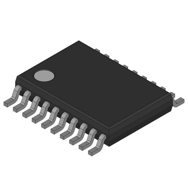
Analog Devices Inc./Maxim Integrated DS2119M
- Part No.:
- DS2119M
- Manufacturer:
- Analog Devices Inc./Maxim Integrated
- Category:
- Signal Terminators
- Package:
- 28-TSSOP (0.173", 4.40mm Width)
- Datasheet:
-
 DS2119M.pdf
- Description:
- IC TERM SCSI LVD/SE ULT3 28TSSOP
- Quantity:
- Payment:

- Shipping:

Inventory:1,055
Please send an inquiry. Send us your inquiry, and we will respond immediately.
Product details
Overview
DS2119M from Maxim Integrated is an Ultra3 multimode SCSI terminator supporting both low-voltage differential (LVD) and single-ended (SE) bus configurations, with automatic mode detection via DIFFSENSE voltage sensing, 110Ω SE termination resistance, 105Ω differential impedance in LVD mode, and HVD isolation capability. It enables backward-compatible SCSI-3/4 bus termination in storage subsystems and server backplanes.
For engineers reviewing the DS2119M datasheet, DS2119M pinout, DS2119M application, or DS2119M equivalent, key selection criteria include its trinary DIFFSENS decoding (SE/LVD/HVD), thermal shutdown protection, 3pF output capacitance, autoselecting termination logic, and TSSOP-28 package compatibility with wide SCSI bus layouts.
Technical Context
The DS2119M implements trinary-mode SCSI bus detection using two comparators and a NAND gate to interpret DIFFSENS voltage levels: <0.6V (SE), 0.7–1.9V (LVD), or >2.4V (HVD). Its internal bandgap reference generates 1.25V for LVD and 2.85V for SE termination regulation.
In LVD mode, it delivers 105Ω differential and 150Ω common-mode termination using laser-trimmed resistor strings and dual current sources; in SE mode, it provides active 110Ω termination with 2.85V quiescent bias and 22mA sink capability per line, while ISO=1 isolates termination pins during HVD detection or thermal shutdown.
Key Specifications
| Parameter | Value and Actual Design Meaning |
|---|---|
| Termination Modes | LVD, SE, and HVD isolation - enables interoperability across legacy SE, modern LVD, and high-voltage differential SCSI devices |
| SE Termination Resistance | 104.5–115.5Ω ±5% - ensures stable 110Ω matching to SCSI-2/3 SE bus impedance |
| LVD Differential Impedance | 100–110Ω - maintains signal integrity on Ultra160/Ultra320 differential buses |
| DIFFSENSE Detection Range | Three-level voltage window: SE (<0.6V), LVD (0.7–1.9V), HVD (>2.4V) - eliminates external RC filtering |
| Output Capacitance | 3pF - minimizes signal reflection and timing skew on high-speed SCSI lines |
| Thermal Shutdown Threshold | 150°C - disables termination and isolates bus pins to prevent damage during overtemperature events |
| Supply Voltage Range | TPWR: 2.7–5.5V (LVD), 4.0–5.5V (SE) - supports mixed-voltage SCSI backplane power domains |
Pinout & Package
DS2119M is housed in a 28-pin TSSOP (0.173") package with exposed heat-sink ground pad (pins 6 and 22). Pin functions are validated per Maxim DS2119M datasheet Rev 010406.
| Pin/Terminal | Circuit Role | Design Meaning |
|---|---|---|
| VREF (Pin 1) | Reference voltage output | Provides 2.85V in SE mode or 1.25V in LVD mode; requires 4.7µF decoupling for regulation stability |
| RxP/RxN (Pins 2–5, 7–12, 18–21, 23–26) | Signal termination terminals | Connect directly to nine SCSI signal line pairs; enable bidirectional LVD/SE termination |
| ISO (Pin 13) | Isolation control input | High = disconnects RxP/RxN from bus during HVD detection or thermal shutdown |
| GND (Pin 14) | Signal ground reference | Primary return path for termination currents and reference circuitry |
| MSTR/SLV (Pin 15) | Mode-select control | High = enables DIFFSENSE driver output for bus master arbitration |
| DIFFSENSE (Pin 16) | Differential mode driver output | Drives SCSI DIFFSENS line when MSTR/SLV = 1; outputs 1.2–1.4V with 5–15mA source capability |
| DIFF_CAP (Pin 17) | Differential mode sense input | Accepts 0.1µF capacitor for internal digital noise filtering of DIFFSENS line |
| TPWR (Pins 27, 28) | Termination power input | Connects to SCSI TERMPWR; requires local 2.2µF + 0.01µF bypassing |
Key Features
| Feature | Design Value |
|---|---|
| Trinary DIFFSENS decoding | Eliminates need for external RC filter by digitally distinguishing SE/LVD/HVD bus states |
| Autoselecting termination logic | Switches between SE and LVD modes without firmware or external control based on real-time bus voltage |
| Fail-safe LVD bias | Maintains 112mV differential bias when no drivers are active, preventing floating bus states |
| HVD isolation mode | Disables termination connection upon HVD detection (DIFFSENS >2.4V), protecting LVD/SE circuitry |
| Thermal shutdown with pin isolation | At 150°C, disables DIFFSENSE driver and isolates RxP/RxN while keeping VREF active |
Applications
| SCSI Server Backplane Termination | Legacy Storage Controller Interface |
|---|---|
Use Scenario: Wide Ultra320 SCSI backplane in 1U/2U rack servers requiring hot-plug support and mixed-device compatibility. IC Role / Device Role / Timing Role: Active multimode terminator managing termination impedance and bus mode signaling for up to nine signal pairs. Use Value: Enables seamless integration of new LVD drives with older SE peripherals without manual jumper configuration or bus reconfiguration. | Use Scenario: Industrial RAID controller board connecting to legacy tape libraries and disk enclosures with varying SCSI standards. IC Role / Device Role / Timing Role: Bus-mode-aware termination device that senses and adapts to connected device types in real time. Use Value: Reduces BOM count by replacing discrete SE and LVD terminators with one auto-configuring component. |
| SCSI Hot-Swap Expansion Chassis | Embedded SCSI Boot Module |
Use Scenario: Modular storage chassis supporting hot insertion of LVD and SE modules without bus reset or reinitialization. IC Role / Device Role / Timing Role: Real-time DIFFSENS monitor and termination switch ensuring stable bus electrical characteristics during dynamic device changes. Use Value: Prevents signal reflections and bus lockup during hot-swap events via sub-100ns mode detection and isolation response. | Use Scenario: Compact embedded system booting from SCSI-connected flash or EEPROM modules in ruggedized environments. IC Role / Device Role / Timing Role: Low-capacitance (3pF), thermally protected terminator placed adjacent to SCSI connector for minimal trace length. Use Value: Ensures reliable boot initialization under temperature stress by maintaining termination integrity up to 70°C ambient. |
Equivalent & Alternatives
The following parts are listed as comparable options for similar SCSI termination applications.
| Alternative Part | Technical Difference | Application Difference | Selection Advice |
|---|---|---|---|
| DS2118M | Single-mode LVD-only terminator; lacks SE termination, DIFFSENSE decoding, and HVD isolation | Requires separate SE terminator for mixed-bus systems; not suitable for legacy compatibility | Select DS2119M when bus may contain SE devices or require automatic mode switching |
| MAX3219E | RS-232 transceiver with integrated charge-pump; no SCSI termination functionality or DIFFSENS interface | Designed for serial communication, not parallel SCSI bus termination | Not functionally comparable; DS2119M serves a distinct SCSI physical layer role |
Compared with DS2119M, DS2118M offers lower cost but no SE support or HVD isolation, making it unsuitable for mixed-mode environments; MAX3219E belongs to a different interface standard entirely and cannot substitute for SCSI termination.
Availability
DS2119M is available at Aetrix Electronics and suitable for SCSI server backplanes, industrial RAID controllers, hot-swap storage chassis, and embedded SCSI boot modules requiring stable component supply and long-term lifecycle support.
Supply support for DS2119M includes scheduled delivery planning, volume procurement assistance, BOM continuity management, traceable sourcing, and lifecycle availability coordination for OEM customers, industrial embedded developers, connected-device designers, and electronics production programs.
Manufacturer
Maxim Integrated (now part of Analog Devices) designs precision analog, mixed-signal, and power management ICs for industrial, computing, and communications applications.
The DS2119M belongs to Maxim's SCSI interface product line, engineered specifically to resolve multimode termination challenges in evolving parallel SCSI architectures from SPI-2 through Ultra320.
FAQ
What is the primary function of the DS2119M in a SCSI system?
The DS2119M serves as an intelligent multimode terminator for Ultra3 SCSI buses, automatically selecting between low-voltage differential (LVD) and single-ended (SE) termination based on real-time DIFFSENSE voltage detection. It also provides HVD isolation and thermal shutdown protection. The DS2119M ensures signal integrity across mixed-device SCSI environments without manual configuration or external mode-selection circuitry.
How does the DS2119M detect and respond to HVD devices on the SCSI bus?
The DS2119M monitors the DIFFSENS line and identifies HVD presence when the voltage exceeds 2.4V. Upon detection, it asserts the ISO pin internally, isolating all RxP/RxN termination pins from the SCSI bus while maintaining VREF activity. This prevents potential damage or interference between incompatible HVD and LVD/SE circuitry. The DS2119M datasheet confirms this behavior is intrinsic to the DS2119M's design and requires no external intervention.
What decoupling capacitors are required for proper operation of the DS2119M?
The DS2119M requires three critical decoupling capacitors: a 4.7µF capacitor between VREF (Pin 1) and GND, a 2.2µF capacitor plus a 0.01µF ceramic capacitor between TPWR (Pins 27/28) and GND, and a 0.1µF capacitor on DIFF_CAP (Pin 17). These values are specified in the DS2119M datasheet Rev 010406 and are essential for stable reference regulation, TERMPWR filtering, and DIFFSENS noise immunity.
Can the DS2119M be used in a purely single-ended SCSI-2 system?
Yes, the DS2119M fully supports actively negated SE SCSI signals and provides precise 110Ω termination with 2.85V quiescent bias. It meets SCSI-2/3 SE specifications and maintains 22mA sink capability per line while limiting reference voltage shift to under 100mV. The DS2119M operates reliably in pure SE systems and is explicitly qualified for 0°C to +70°C ambient conditions per its ordering information.
What is the purpose of the MSTR/SLV pin on the DS2119M?
The MSTR/SLV pin (Pin 15) configures the DS2119M as either a master or slave terminator on the SCSI bus. When pulled high, it enables the internal DIFFSENSE driver (Pin 16) to actively drive the SCSI DIFFSENS line, allowing the DS2119M to assert bus mode. When low, the DS2119M operates as a non-controlling terminator that only senses DIFFSENS. This function is defined in the DS2119M pin description and functional block diagram.
DS2119M Specifications
- Product attributes
- Attribute value
- Manufacturer:
- Analog Devices Inc./Maxim Integrated
- Series:
- -
- Package/Case:
- 28-TSSOP (0.173", 4.40mm Width)
- Packaging:
- Tube
- Product Status:
- Obsolete
- Type:
- SCSI, LVD, SE
- Number of Terminations:
- 9
- Voltage - Supply:
- 4V ~ 5.5V
- Operating Temperature:
- 0°C ~ 70°C
- Mounting Type:
- Surface Mount
- Supplier Device Package:
- 28-TSSOP
DS2119M FAQ
1.How can I place an order for DS2119M through Aetrix?
Please submit a Request for Quotation (RFQ) for DS2119M on Aetrix. Our sales agent will provide a competitive quotation and guide you through the order confirmation once you accept the terms.
2.Are the price and stock information for DS2119M reliable?
The price and inventory of DS2119M are updated periodically and may fluctuate due to market conditions. Stock and pricing data are typically refreshed every 24 hours. Quotation validity for DS2119M is usually 5 days.
3.What payment methods are accepted for DS2119M?
We accept Wire Transfer, PayPal, Credit Card, Western Union, MoneyGram, and Escrow for DS2119M transactions.
Note: Certain payment methods may incur a processing fee.
4.How is shipping managed for DS2119M?
DS2119M orders can be shipped via leading logistics carriers, including DHL, UPS, FedEx, TNT, or Registered Mail.
Once your DS2119M order is processed, you will receive an email with the shipment details and tracking number.
Note: Tracking information may take up to 24 hours to appear. Express delivery typically takes 3–5 business days.
5.How can I obtain technical support or documentation for DS2119M?
For technical support, including DS2119M datasheets, pinout diagrams, or application guidance, please contact our engineering support team. They can provide detailed documentation and assistance for your DS2119M requirements.
6.How does Aetrix verify that DS2119M is sourced from the original manufacturer or authorized distributors?
All DS2119M products on Aetrix are procured from qualified distributors and authorized channels. Our dedicated quality assurance team conducts strict verification, including traceability checks and, if necessary, third-party testing. This ensures that DS2119M meets industry standards.
7.What is the process for return or replacement of DS2119M?
All DS2119M units undergo pre-shipment inspection (PSI). If there is an issue with DS2119M, returns or replacements are accepted under the following conditions:
1.Quantity discrepancies, incorrect items, or visible external defects (such as breakage or corrosion), acknowledged by Aetrix.
2.The issue is reported within 90 days of delivery.
3.The DS2119M part is unused and in its original packaging.
Return procedure for DS2119M:
1.Submit a request within 90 days.
2.Obtain a Return Material Authorization (RMA) from Aetrix.
DS2119M Tags
-
LTC1344IG#PBF
Analog Devices Inc.
-
LTC1344AIG#PBF
Analog Devices Inc.

-
UCC5672PWP
Texas Instruments
-
LTC1344ACG#PBF
Analog Devices Inc.
-
MXL1344ACAG+
Analog Devices Inc./Maxim Integrated
-
LTC1344CG#PBF
Analog Devices Inc.
-
PACUSB-U3R
onsemi
-
PACUSB-D1Y5R
onsemi
-
FAN1804MCX
Fairchild Semiconductor
-
MCCS142237DT
onsemi
-
MCCS142237DTR2
onsemi

-
UCC5519PWPR
Texas Instruments
Tech Hub

A practical engineering guide to 3.3V and 5V logic compatibility, input thresholds, resistor dividers, translator ICs, MOSFET level shifting, I2C pull-ups, timing limits and power-sequencing risks.

The 74HC595 uses push-pull logic outputs, while the TPIC6B595 uses 50 V open-drain DMOS sinks for higher-power loads. This guide compares timing, current limits, 3.3 V interfacing, load wiring, thermal…

The 74HC595 converts serial data into eight stable parallel outputs. This guide covers pin functions, shift and storage timing, OE and MR behavior, drive-current limits, cascading, voltage compatibilit…

A technical comparison of level-sensitive latches and edge-triggered flip-flops, covering timing windows, setup and hold limits, master–slave operation, time borrowing, race-through, HDL inference and…

A D latch stores one bit while Enable controls when data can pass. This reference covers gate-level operation, truth tables, transparency, setup and hold timing, LE versus OE, common ICs and practical …

An SR latch stores one bit through cross-coupled feedback. This engineering reference covers NOR and NAND implementations, truth tables, forbidden-state recovery, gated operation, switch debouncing, fa…

Latch circuits retain one bit through feedback. This technical reference covers SR and D latches, truth tables, transparency, timing limits, latch-versus-flip-flop behavior, applications and common log…

An engineering guide to LED driver operation, constant-current and constant-voltage outputs, linear and switching topologies, dimming, IC selection, calculations, replacement compatibility, and fault c…

Operational amplifier guide covering op amp basics, feedback, ideal vs real op amps, common configurations, buffer circuits, offset, bias current, gain-bandwidth, slew rate, rail-to-rail limits and sel…

Jumper cables guide covering safe connection order, red and black clamp placement, final ground connection, cable gauge, length, clamp quality, copper vs CCA cables, jump starter comparison and battery…


