
 My Inquiry
 My Account


Analog Devices Inc./Maxim Integrated DS2125/T&R
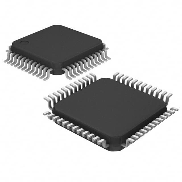
- Part No.:
- DS2125/T&R
- Manufacturer:
- Analog Devices Inc./Maxim Integrated
- Category:
- Signal Terminators
- Package:
- 48-LQFP
- Datasheet:
-
 DS2125/T&R.pdf
- Description:
- IC TERM SCSI ULT3 LVD/SE 48-LQFP
- Quantity:
- Payment:

- Shipping:

Inventory:4,465
Please send an inquiry. Send us your inquiry, and we will respond immediately.
Product details
Overview
DS2125/T&R from Maxim Integrated (formerly Dallas Semiconductor) is a multimode Ultra3 SCSI 15-line terminator supporting both low-voltage differential (LVD) and single-ended (SE) bus configurations. It auto-selects termination mode via DIFFSENSE voltage sensing, delivers 100–110Ω LVD differential impedance and 104.5–115.5Ω SE resistance with ±5% tolerance, and integrates thermal shutdown and hot-plug compatibility for RAID systems and SCSI HBAs.
For engineers reviewing the DS2125/T&R datasheet, DS2125/T&R pinout, DS2125/T&R application, or DS2125/T&R equivalent, key selection considerations include its automatic LVD/SE mode switching, 3pF power-down capacitance, dual VREF regulation (1.25V in LVD / 2.85V in SE), ISO-controlled bus isolation, and 48-pin LQFP package with HS_GND thermal pad.
Technical Context
The DS2125/T&R implements trinary DIFFSENS decoding using two comparators and a NAND gate to distinguish SE (<0.6V), HVD (0.7–1.9V), and LVD (2.4–VTPWR+0.3V) bus conditions. Its control logic dynamically selects between 1.25V and 2.85V reference voltages and reconfigures precision resistor strings accordingly.
LVD termination uses two current sources with laser-trimmed 15-resistor strings yielding 105Ω differential and 150Ω common-mode impedance; SE mode employs a 2.85V regulator driving 15×110Ω resistors with active ground-switching on RP pins and -22.4mA termination current at 0.5V signal level.
Key Specifications
| Parameter | Value and Actual Design Meaning |
|---|---|
| LVD Differential Resistance | 100–110Ω - ensures impedance matching for Ultra3 LVD SCSI signaling integrity |
| SE Termination Resistance | 104.5–115.5Ω - maintains 110Ω nominal with ±5% tolerance for legacy SE device compatibility |
| Mode Switch Delay | 0.66–2.00ms - provides stable bus mode detection without transient glitches during hot-plug events |
| Power-Down Capacitance | 3pF - minimizes signal reflection and timing skew on high-speed SCSI lines |
| Thermal Shutdown Threshold | 150°C - protects against sustained overtemperature in dense storage enclosures |
| Supply Current (LVD) | 20–32mA - enables low-power operation when only LVD devices are present on the bus |
| VREF Regulation | 1.25V (LVD) / 2.85V (SE) - supplies precise bias references for respective termination topologies |
Pinout & Package
The DS2125/T&R is housed in a 48-pin LQFP (1.4mm height) with exposed thermal pad connected internally to HS_GND pins. The package supports automated tape-and-reel handling and RoHS compliance (lead-free marking "+" on top).
| Pin/Terminal | Circuit Role | Design Meaning |
|---|---|---|
| RxP/RxN (1,2,11–26,37–48) | SCSI Signal Termination | 15 differential pairs (30 pins) directly connect to SCSI bus lines for bidirectional termination |
| TPWR (Pin 3) | Termination Power Input | Accepts TERMPWR (3.3–5.5V) with mandatory 2.2µF local decoupling for stable bias delivery |
| VREF (Pin 10) | Reference Voltage Output | Provides 1.25V (LVD) or 2.85V (SE); requires 4.7µF capacitor to ground for regulation stability |
| DIFFSENSE (Pin 35) | DIFFSENS Bus Driver | Actively drives SCSI DIFFSENS line to declare bus mode; sinks 100–200µA at 3.3V |
| DIFF_CAP (Pin 34) | DIFFSENS Filter Input | Connects to 0.1µF capacitor for noise filtering; senses bus mode via voltage window detection |
| ISO (Pin 36) | Isolation Control | High-level input disables RxP/RxN connection to bus while keeping VREF active; internal pulldown defaults to termination |
| GND (Pin 27) | Signal Ground Reference | Primary 0V reference for analog circuitry; separate from HS_GND thermal plane |
| HS_GND (Pins 4–9,28–33) | Heat-Sink Ground | Internally tied to exposed thermal pad; must be soldered to PCB ground plane for thermal management |
Key Features
| Feature | Design Value |
|---|---|
| Auto-Mode Selection | Trinary DIFFSENS decoding (SE/HVD/LVD) enables zero-configuration bus compatibility across mixed-device environments |
| Dual VREF Regulation | Integrated 1.25V (LVD) and 2.85V (SE) regulators eliminate external reference ICs and reduce BOM count |
| Hot-Plug Safety | Thermal shutdown + ISO-controlled isolation prevent bus disruption during live insertion/removal of SCSI peripherals |
| Low Signal Loading | 3pF pin capacitance preserves signal edge rates up to Ultra3's 80MB/s transfer rate without added termination delay |
| Fail-Safe Bias | 112mV differential bias in LVD mode maintains bus readiness when no drivers are active, preventing floating line states |
Applications
| Raid Systems | SCSI Host Bus Adapter (HBA) Cards |
|---|---|
Use Scenario: High-availability storage arrays requiring simultaneous support for legacy SE and modern LVD SCSI drives. IC Role / Device Role / Timing Role: Multimode terminator ensuring impedance continuity across mixed-speed, mixed-signaling SCSI backplanes. Use Value: Eliminates manual jumper configuration and prevents bus termination errors that cause data corruption or link failure. | Use Scenario: Add-in cards connecting servers to external SCSI storage enclosures with varying device generations. IC Role / Device Role / Timing Role: Bus interface conditioner providing automatic signal integrity management at the host controller boundary. Use Value: Enables plug-and-play interoperability between Ultra3 HBAs and older SE-only JBODs without firmware updates. |
| Servers | Network Attached Storage (NAS) |
Use Scenario: Enterprise rack-mount servers with internal wide SCSI buses hosting both LVD tape libraries and SE disk subsystems. IC Role / Device Role / Timing Role: System-level termination manager maintaining signal fidelity across long, branched SCSI traces under thermal stress. Use Value: Prevents intermittent timeouts and CRC errors caused by impedance mismatch in thermally constrained chassis environments. | Use Scenario: Consumer/prosumer NAS units integrating legacy SCSI scanners or CD-ROMs alongside newer LVD hard drives. IC Role / Device Role / Timing Role: Embedded termination node enabling cost-effective reuse of existing SCSI peripheral designs. Use Value: Reduces bill-of-materials cost by avoiding separate SE and LVD termination solutions in dual-mode storage platforms. |
Equivalent & Alternatives
The following parts are listed as comparable options for similar SCSI termination applications.
| Alternative Part | Technical Difference | Application Difference | Selection Advice |
|---|---|---|---|
| DS2124 | 16-pin SOIC; supports only SE termination; no LVD capability or DIFFSENSE circuitry | Limited to legacy-only SCSI systems without LVD devices | Select DS2124 only when bus composition is fixed SE and board space constraints prohibit 48-pin LQFP |
| MAX3202E | 32-pin TQFN; supports LVD/SE but lacks integrated DIFFSENSE driver and thermal shutdown | Requires external mode-detection logic and thermal monitoring circuitry | Choose MAX3202E only if system-level DIFFSENSE control is already implemented and thermal protection is handled externally |
Compared with DS2125/T&R, DS2124 offers compact SE-only termination but no multimode flexibility, while MAX3202E provides LVD/SE support in smaller footprint yet demands additional external components for full Ultra3 compliance-making DS2125/T&R the only single-chip solution with integrated DIFFSENSE drive, thermal shutdown, and auto-mode switching.
Availability
DS2125/T&R is available at Aetrix Electronics and suitable for RAID systems, SCSI host bus adapter (HBA) cards, and enterprise servers requiring stable component supply, long-term lifecycle support, and guaranteed RoHS-compliant sourcing.
Supply support for DS2125/T&R includes scheduled delivery planning, volume procurement assistance, BOM continuity management, traceable sourcing, and lifecycle availability coordination for OEM customers, industrial embedded developers, connected-device designers, and electronics production programs.
Manufacturer
Maxim Integrated (acquired Dallas Semiconductor in 2011) is a U.S.-based analog and mixed-signal semiconductor company specializing in high-reliability interface, power, and timing solutions.
The DS2125/T&R belongs to Maxim's legacy SCSI interface product line, designed specifically to simplify termination design in mixed-generation parallel SCSI storage systems while meeting Ultra3 specification requirements.
FAQ
What is the primary function of the DS2125/T&R in a SCSI system?
The DS2125/T&R serves as an intelligent multimode terminator for Ultra3 SCSI buses, automatically selecting between low-voltage differential (LVD) and single-ended (SE) termination based on the DIFFSENS line voltage. It ensures proper impedance matching across 15 signal line pairs, maintains fail-safe bias levels, and supports hot-plug operations without manual configuration-critical for reliable data transfer in mixed-device storage environments where DS2125/T&R operates as the sole termination IC per bus segment.
How does the DS2125/T&R detect whether the SCSI bus is operating in LVD or SE mode?
The DS2125/T&R detects bus mode through its DIFFSENSE and DIFF_CAP pins using trinary voltage window detection: SE mode is identified when DIFFSENS voltage is below 0.6V, HVD when between 0.7V–1.9V, and LVD when above 2.4V. This is implemented via two internal comparators and a NAND gate within DS2125/T&R, enabling autonomous mode switching without external microcontroller intervention or configuration registers.
What are the required external components for proper operation of the DS2125/T&R?
The DS2125/T&R requires three mandatory external components: a 2.2µF capacitor between TPWR and ground for power rail decoupling, a 4.7µF capacitor between VREF and ground to stabilize reference voltage regulation, and a 0.1µF capacitor between DIFF_CAP and ground to filter noise on the DIFFSENS sense line. These capacitors must be placed as close as possible to their respective pins to ensure signal integrity and thermal stability in DS2125/T&R applications.
Does the DS2125/T&R support hot-plug functionality, and how is it implemented?
Yes, the DS2125/T&R supports SCSI bus hot-plug via integrated thermal shutdown circuitry (triggering at 150°C with 10°C hysteresis) and ISO-controlled isolation. When ISO is pulled high or thermal shutdown activates, DS2125/T&R disconnects its RxP/RxN pins from the bus while maintaining VREF output, preventing signal disruption during live insertion or removal of SCSI peripherals-ensuring continuous operation of DS2125/T&R in mission-critical storage systems.
What is the significance of the HS_GND pins on the DS2125/T&R package?
The HS_GND pins (Pins 4–9 and 28–33) are internally connected to the exposed thermal pad of the 48-pin LQFP package and serve as dedicated heat-sink ground connections. They must be soldered to a large PCB copper pour tied to system ground to dissipate up to 2W of power and maintain junction temperature below 150°C. Proper HS_GND layout is essential for DS2125/T&R reliability in high-density server and RAID applications where thermal management directly impacts termination accuracy and longevity.
DS2125/T&R Specifications
- Product attributes
- Attribute value
- Manufacturer:
- Analog Devices Inc./Maxim Integrated
- Series:
- -
- Package/Case:
- 48-LQFP
- Packaging:
- Tape & Reel (TR)
- Product Status:
- Obsolete
- Type:
- SCSI, LVD, SE
- Number of Terminations:
- 15
- Voltage - Supply:
- 2.7V ~ 5.5V
- Operating Temperature:
- 0°C ~ 70°C
- Mounting Type:
- Surface Mount
- Supplier Device Package:
- 48-LQFP (7x7)
DS2125/T&R FAQ
1.How can I place an order for DS2125/T&R through Aetrix?
Please submit a Request for Quotation (RFQ) for DS2125/T&R on Aetrix. Our sales agent will provide a competitive quotation and guide you through the order confirmation once you accept the terms.
2.Are the price and stock information for DS2125/T&R reliable?
The price and inventory of DS2125/T&R are updated periodically and may fluctuate due to market conditions. Stock and pricing data are typically refreshed every 24 hours. Quotation validity for DS2125/T&R is usually 5 days.
3.What payment methods are accepted for DS2125/T&R?
We accept Wire Transfer, PayPal, Credit Card, Western Union, MoneyGram, and Escrow for DS2125/T&R transactions.
Note: Certain payment methods may incur a processing fee.
4.How is shipping managed for DS2125/T&R?
DS2125/T&R orders can be shipped via leading logistics carriers, including DHL, UPS, FedEx, TNT, or Registered Mail.
Once your DS2125/T&R order is processed, you will receive an email with the shipment details and tracking number.
Note: Tracking information may take up to 24 hours to appear. Express delivery typically takes 3–5 business days.
5.How can I obtain technical support or documentation for DS2125/T&R?
For technical support, including DS2125/T&R datasheets, pinout diagrams, or application guidance, please contact our engineering support team. They can provide detailed documentation and assistance for your DS2125/T&R requirements.
6.How does Aetrix verify that DS2125/T&R is sourced from the original manufacturer or authorized distributors?
All DS2125/T&R products on Aetrix are procured from qualified distributors and authorized channels. Our dedicated quality assurance team conducts strict verification, including traceability checks and, if necessary, third-party testing. This ensures that DS2125/T&R meets industry standards.
7.What is the process for return or replacement of DS2125/T&R?
All DS2125/T&R units undergo pre-shipment inspection (PSI). If there is an issue with DS2125/T&R, returns or replacements are accepted under the following conditions:
1.Quantity discrepancies, incorrect items, or visible external defects (such as breakage or corrosion), acknowledged by Aetrix.
2.The issue is reported within 90 days of delivery.
3.The DS2125/T&R part is unused and in its original packaging.
Return procedure for DS2125/T&R:
1.Submit a request within 90 days.
2.Obtain a Return Material Authorization (RMA) from Aetrix.
DS2125/T&R Tags
-
LTC1344IG#PBF
Analog Devices Inc.
-
LTC1344AIG#PBF
Analog Devices Inc.

-
UCC5672PWP
Texas Instruments
-
LTC1344ACG#PBF
Analog Devices Inc.
-
MXL1344ACAG+
Analog Devices Inc./Maxim Integrated
-
LTC1344CG#PBF
Analog Devices Inc.
-
PACUSB-U3R
onsemi
-
PACUSB-D1Y5R
onsemi
-
FAN1804MCX
Fairchild Semiconductor
-
MCCS142237DT
onsemi
-
MCCS142237DTR2
onsemi

-
UCC5519PWPR
Texas Instruments
Tech Hub

A practical engineering guide to 3.3V and 5V logic compatibility, input thresholds, resistor dividers, translator ICs, MOSFET level shifting, I2C pull-ups, timing limits and power-sequencing risks.

The 74HC595 uses push-pull logic outputs, while the TPIC6B595 uses 50 V open-drain DMOS sinks for higher-power loads. This guide compares timing, current limits, 3.3 V interfacing, load wiring, thermal…

The 74HC595 converts serial data into eight stable parallel outputs. This guide covers pin functions, shift and storage timing, OE and MR behavior, drive-current limits, cascading, voltage compatibilit…

A technical comparison of level-sensitive latches and edge-triggered flip-flops, covering timing windows, setup and hold limits, master–slave operation, time borrowing, race-through, HDL inference and…

A D latch stores one bit while Enable controls when data can pass. This reference covers gate-level operation, truth tables, transparency, setup and hold timing, LE versus OE, common ICs and practical …

An SR latch stores one bit through cross-coupled feedback. This engineering reference covers NOR and NAND implementations, truth tables, forbidden-state recovery, gated operation, switch debouncing, fa…

Latch circuits retain one bit through feedback. This technical reference covers SR and D latches, truth tables, transparency, timing limits, latch-versus-flip-flop behavior, applications and common log…

An engineering guide to LED driver operation, constant-current and constant-voltage outputs, linear and switching topologies, dimming, IC selection, calculations, replacement compatibility, and fault c…

Operational amplifier guide covering op amp basics, feedback, ideal vs real op amps, common configurations, buffer circuits, offset, bias current, gain-bandwidth, slew rate, rail-to-rail limits and sel…

Jumper cables guide covering safe connection order, red and black clamp placement, final ground connection, cable gauge, length, clamp quality, copper vs CCA cables, jump starter comparison and battery…


