
 My Inquiry
 My Account


Analog Devices Inc./Maxim Integrated DS21554LN+
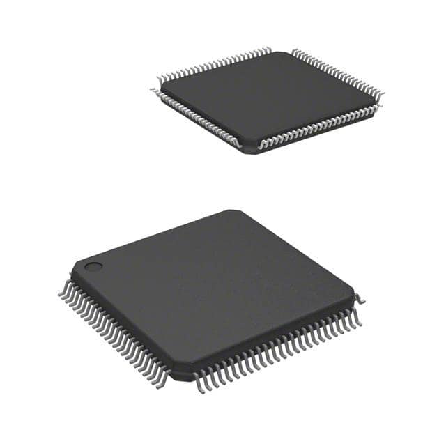
- Part No.:
- DS21554LN+
- Manufacturer:
- Analog Devices Inc./Maxim Integrated
- Category:
- Telecom
- Package:
- 100-LQFP
- Datasheet:
-
 DS21554LN+.pdf
- Description:
- IC TELECOM INTERFACE 100LQFP
- Quantity:
- Payment:

- Shipping:

Inventory:3,567
Please send an inquiry. Send us your inquiry, and we will respond immediately.
Product details
Overview
DS21554LN+ from Maxim Integrated is a 5V E1 single-chip transceiver (SCT) designed for CEPT PCM-30/ISDN-PRI line interface applications. It performs clock/data recovery from AMI/HDB3 E1 waveforms, provides 32-bit or 128-bit crystal-less jitter attenuation, supports G.703-compliant waveshaping for 75Ω coax and 120Ω twisted-pair, and operates across -40°C to +85°C in a 100-pin LQFP package.
For engineers reviewing the DS21554LN+ datasheet, DS21554LN+ pinout, DS21554LN+ application, or DS21554LN+ equivalent, key selection criteria include E1 framer functionality with FAS/CAS/CCS/CRC4 support, dual elastic store slip buffers for asynchronous backplane interfacing up to 8.192MHz, IEEE 1149.1 JTAG boundary scan capability, and programmable output clocks for fractional E1, H0, and H12 systems.
Technical Context
The DS21554LN+ integrates independent transmit and receive paths with full framer/formatter logic, enabling simultaneous frame alignment, multiframe synchronization, and signaling data extraction/insertion (CAS, Si, Sa bits). Its on-chip jitter attenuator is configurable for either path and selectable between 32-bit or 128-bit depth, supporting compliance with ITU-T G.823 jitter tolerance requirements.
It features an 8-bit parallel control port compatible with both Intel- and Motorola-style buses (multiplexed or nonmultiplexed), direct access to internal registers for real-time configuration, and hardware-based signaling with freeze interrupt generation. The device supports protected line interfaces per ETS 300 011/233 and includes four distinct loopback modes for comprehensive system-level testing.
Key Specifications
| Parameter | Value and Actual Design Meaning |
|---|---|
| Supply Voltage | 5V ±5% - enables direct integration into legacy 5V telecom infrastructure without level-shifting. |
| Operating Temperature | -40°C to +85°C - qualified for industrial and outdoor base station environments. |
| Jitter Attenuation Depth | Selectable 32-bit or 128-bit - determines phase noise suppression bandwidth and holdover stability during line interruptions. |
| Elastic Store Clock Range | Up to 8.192MHz - allows seamless connection to asynchronous backplanes including TDM switch fabrics. |
| Receive Sensitivity | 0 to -43dB - supports operation over 2km of 22AWG twisted-pair cable without repeaters. |
| Standards Compliance | ITU-T G.703/G.704/G.706/G.823/G.732/I.431; ETS 300 011/233/166; CTR12/CTR4 - ensures interoperability in global E1 networks. |
| HDLC Buffer Size | 64-byte - sufficient for Sa-bit link framing or full DS0 channel HDLC encapsulation. |
Pinout & Package
DS21554LN+ is housed in a 100-pin LQFP package (14mm × 14mm, 0.5mm pitch), thermally optimized for telecom line card applications with exposed thermal pad. Pin assignments are fully documented in Maxim's DS21354/DS21554 datasheet Section 3.1.
| Pin/Terminal | Circuit Role | Design Meaning |
|---|---|---|
| RRING / RTIP | Receive Line Interface Inputs | Differential analog inputs for transformer-coupled E1 AMI/HDB3 waveform; support line build-out (LBO) up to 2km. |
| TRING / TTIP | Transmit Line Interface Outputs | Differential outputs driving 75Ω coax or 120Ω twisted-pair per G.703; include current limiting for short-circuit protection. |
| RSYSCLK / TSYSCLK | Asynchronous Backplane Clock Inputs | Accept 1.544MHz, 2.048MHz, 4.096MHz, or 8.192MHz clocks to synchronize elastic stores with backplane timing domains. |
| D0–D7 | Parallel Control Port Data Bus | 8-bit bidirectional bus supporting Intel/Motorola timing; enables single controller to manage multiple E1 lines via register addressing. |
| TMS / TCK / TDI / TDO | JTAG Test Access Port | IEEE 1149.1-compliant boundary scan interface for production test, debug, and in-system verification. |
Key Features
| Feature | Design Value |
|---|---|
| Crystal-less jitter attenuation | Eliminates external crystal requirement while maintaining G.823-compliant jitter performance in transmit or receive path. |
| Dual two-frame elastic store buffers | Enables robust synchronization between recovered E1 timing and asynchronous backplane clocks up to 8.192MHz. |
| Interleaved PCM bus operation | Supports byte- or frame-interleave modes for efficient time-slot multiplexing across multiple SCTs in high-density line cards. |
| Hardware-based CAS signaling | Extracts and inserts channel-associated signaling without CPU intervention, reducing host processor load in real-time systems. |
| Four independent loopback functions | Includes framer, remote, local, and per-channel loopbacks - essential for layered diagnostics from physical layer to signaling layer. |
Applications
| E1 Line Card Interface | ISDN-PRI Gateway |
|---|---|
Use Scenario: Integration into carrier-grade E1 line interface cards for central office or remote terminal equipment. IC Role / Device Role / Timing Role: Full E1 transceiver handling clock recovery, framing, signaling, and waveshaping - acts as the physical layer bridge between line and backplane. Use Value: Eliminates need for discrete framer, jitter cleaner, and line driver ICs, reducing BOM count and board area by >40% versus multi-chip solutions. | Use Scenario: Deployment in ISDN Primary Rate Interface gateways connecting PSTN to VoIP or PBX systems. IC Role / Device Role / Timing Role: Provides CAS and CCS signaling support, Sa/Si bit access, and HDLC-controlled DS0 channels for protocol translation. Use Value: Enables simultaneous handling of 30 voice/data channels plus signaling in a single 100-pin LQFP, simplifying gateway architecture and lowering latency. |
| HDSL/E1 Repeater Unit | Network Monitoring Tap |
Use Scenario: Use in HDSL-based E1 repeater units extending reach beyond standard 2km limits. IC Role / Device Role / Timing Role: Performs line interface decoupling - processes NRZ data streams independently of framer logic for transparent signal regeneration. Use Value: Allows "tap" of bipolar data before/after framer, enabling in-band monitoring and error injection without disrupting live traffic. | Use Scenario: Embedded in passive network monitoring probes for E1 traffic analysis and alarm detection. IC Role / Device Role / Timing Role: Operates in receive monitor mode with gain-adjustable analog front-end to capture line signals without affecting primary path integrity. Use Value: Delivers real-time RLOS, AIS, RRA, and RAIS alarm detection with interrupt-on-change, enabling rapid fault isolation in managed networks. |
Equivalent & Alternatives
The following parts are listed as comparable options for similar E1 transceiver applications.
| Alternative Part | Technical Difference | Application Difference | Selection Advice |
|---|---|---|---|
| DS21554L | Same silicon, 0°C to +70°C temperature range; identical pinout and register map. | Not suitable for extended-temperature industrial or outdoor deployments. | Select DS21554L only for commercial-temperature indoor equipment where cost optimization is prioritized over environmental robustness. |
| DS21354LN+ | 3.3V supply version; shares same feature set, pinout, and software compatibility but requires different power rail design. | Targeted at newer low-power telecom platforms; lacks 5V tolerance on I/O pins. | Choose DS21354LN+ when migrating to 3.3V infrastructure or when lower power consumption (<350mW typical) is critical. |
Compared with DS21554L and DS21354LN+, the DS21554LN+ uniquely delivers 5V operation with industrial temperature range and full backward compatibility with DS2154/DS2152 pinouts - making it the preferred choice for retrofitting legacy 5V E1 line cards requiring extended thermal reliability.
Availability
DS21554LN+ is available at Aetrix Electronics and suitable for E1 line interface cards, ISDN-PRI gateways, HDSL repeaters, and telecom network monitoring equipment requiring stable component supply across extended temperature ranges and long product lifecycles.
Supply support for DS21554LN+ includes scheduled delivery planning, volume procurement assistance, BOM continuity management, traceable sourcing, and lifecycle availability coordination for OEM customers, industrial embedded developers, connected-device designers, and electronics production programs.
Manufacturer
Maxim Integrated (now part of Analog Devices) is a U.S.-based semiconductor company specializing in precision analog, mixed-signal, and high-reliability interface ICs for communications, industrial, and automotive markets.
The DS21554LN+ belongs to Maxim's E1/T1 transceiver product line, engineered specifically for CEPT-compliant telecommunications infrastructure where deterministic timing, standards compliance, and field-proven reliability are mandatory.
FAQ
What is the operating voltage range for DS21554LN+?
The DS21554LN+ operates at a nominal 5V supply with ±5% tolerance (4.75V to 5.25V). This fixed 5V requirement distinguishes it from the 3.3V DS21354LN+ variant and ensures compatibility with legacy telecom power architectures. All I/O pins are 5V-tolerant, and the device draws approximately 420mW typical power under full E1 load. DS21554LN+ does not support dual-supply or voltage scaling modes.
Does DS21554LN+ support both FAS and CRC4 multiframe formats?
Yes, DS21554LN+ fully supports both FAS (Frame Alignment Signal) and CRC4 (Cyclical Redundancy Check) multiframe formats, as required by ITU-T G.704 and G.706. The framer automatically detects and locks to either format, and internal registers allow software-selectable configuration for CAS, CCS, or Sa-bit operation within each. DS21554LN+ also provides full access to Si and Sa bits aligned with CRC-4 multiframe boundaries for international signaling applications.
Can DS21554LN+ be used with asynchronous backplane clocks?
Yes, DS21554LN+ includes dual independent elastic store buffers - one on the receive side and one on the transmit side - each accepting RSYSCLK or TSYSCLK inputs up to 8.192MHz. These buffers absorb phase and frequency differences between recovered E1 timing and asynchronous backplane clocks, enabling reliable interconnection to TDM switches, DSPs, or FPGA-based fabric without external clock domain crossing logic. DS21554LN+ supports both byte- and frame-interleave PCM bus modes for multi-SCT synchronization.
Is DS21554LN+ pin-compatible with older Maxim E1 transceivers?
Yes, DS21554LN+ is explicitly pin-compatible with DS2154, DS2152, DS21352, and DS21552 single-chip transceivers, as confirmed in the datasheet Feature list and Pin Configuration section. This allows drop-in replacement in existing designs without PCB layout changes. DS21554LN+ retains identical pin functions, package dimensions (100-pin LQFP), and register mapping - ensuring full hardware and software compatibility with legacy DS2154-based systems.
What line interface standards does DS21554LN+ comply with?
DS21554LN+ complies with ITU-T G.703 (physical layer waveshaping), G.704 (framing structure), G.706 (error detection), G.823 (jitter generation/tolerance), G.732 (line build-out), and I.431 (ISDN-PRI); plus ETSI standards 300 011, 300 233, and 300 166, and CTR12/CTR4. It meets all electrical and timing requirements for 75Ω coax and 120Ω twisted-pair E1 interfaces, including short-circuit current limiting and protected interface operation per ETS 300 233.
DS21554LN+ Specifications
- Product attributes
- Attribute value
- Manufacturer:
- Analog Devices Inc./Maxim Integrated
- Series:
- -
- Package/Case:
- 100-LQFP
- Packaging:
- Tray
- Product Status:
- Active
- Function:
- Single-Chip Transceiver
- Interface:
- E1, HDLC, J1, T1
- Number of Circuits:
- 1
- Voltage - Supply:
- 4.75V ~ 5.25V
- Current - Supply:
- 75mA
- Power (Watts):
- -
- Operating Temperature:
- -40°C ~ 85°C
- Grade:
- -
- Qualification:
- -
- Mounting Type:
- Surface Mount
- Supplier Device Package:
- 100-LQFP (14x14)
DS21554LN+ FAQ
1.How can I place an order for DS21554LN+ through Aetrix?
Please submit a Request for Quotation (RFQ) for DS21554LN+ on Aetrix. Our sales agent will provide a competitive quotation and guide you through the order confirmation once you accept the terms.
2.Are the price and stock information for DS21554LN+ reliable?
The price and inventory of DS21554LN+ are updated periodically and may fluctuate due to market conditions. Stock and pricing data are typically refreshed every 24 hours. Quotation validity for DS21554LN+ is usually 5 days.
3.What payment methods are accepted for DS21554LN+?
We accept Wire Transfer, PayPal, Credit Card, Western Union, MoneyGram, and Escrow for DS21554LN+ transactions.
Note: Certain payment methods may incur a processing fee.
4.How is shipping managed for DS21554LN+?
DS21554LN+ orders can be shipped via leading logistics carriers, including DHL, UPS, FedEx, TNT, or Registered Mail.
Once your DS21554LN+ order is processed, you will receive an email with the shipment details and tracking number.
Note: Tracking information may take up to 24 hours to appear. Express delivery typically takes 3–5 business days.
5.How can I obtain technical support or documentation for DS21554LN+?
For technical support, including DS21554LN+ datasheets, pinout diagrams, or application guidance, please contact our engineering support team. They can provide detailed documentation and assistance for your DS21554LN+ requirements.
6.How does Aetrix verify that DS21554LN+ is sourced from the original manufacturer or authorized distributors?
All DS21554LN+ products on Aetrix are procured from qualified distributors and authorized channels. Our dedicated quality assurance team conducts strict verification, including traceability checks and, if necessary, third-party testing. This ensures that DS21554LN+ meets industry standards.
7.What is the process for return or replacement of DS21554LN+?
All DS21554LN+ units undergo pre-shipment inspection (PSI). If there is an issue with DS21554LN+, returns or replacements are accepted under the following conditions:
1.Quantity discrepancies, incorrect items, or visible external defects (such as breakage or corrosion), acknowledged by Aetrix.
2.The issue is reported within 90 days of delivery.
3.The DS21554LN+ part is unused and in its original packaging.
Return procedure for DS21554LN+:
1.Submit a request within 90 days.
2.Obtain a Return Material Authorization (RMA) from Aetrix.
DS21554LN+ Tags

-
LMC567CMX/NOPB
Texas Instruments
-
LM567CMX/NOPB
Texas Instruments
-
LM567CM/NOPB
Texas Instruments

-
VSC8531XMW-02
Microchip Technology
-
VSC8531XMW-05
Microchip Technology

-
GPY115C0VI
MaxLinear, Inc.

-
SI32185-A-FMR
Skyworks Solutions Inc.

-
VSC8541XMV-05
Microchip Technology

-
SI32178-B-FM1R
Skyworks Solutions Inc.
-
GPY215C0VI
MaxLinear, Inc.

-
CPC7514ZTR
Littelfuse Inc.

-
VSC8502XML-03
Microchip Technology
Tech Hub

A practical engineering guide to 3.3V and 5V logic compatibility, input thresholds, resistor dividers, translator ICs, MOSFET level shifting, I2C pull-ups, timing limits and power-sequencing risks.

The 74HC595 uses push-pull logic outputs, while the TPIC6B595 uses 50 V open-drain DMOS sinks for higher-power loads. This guide compares timing, current limits, 3.3 V interfacing, load wiring, thermal…

The 74HC595 converts serial data into eight stable parallel outputs. This guide covers pin functions, shift and storage timing, OE and MR behavior, drive-current limits, cascading, voltage compatibilit…

A technical comparison of level-sensitive latches and edge-triggered flip-flops, covering timing windows, setup and hold limits, master–slave operation, time borrowing, race-through, HDL inference and…

A D latch stores one bit while Enable controls when data can pass. This reference covers gate-level operation, truth tables, transparency, setup and hold timing, LE versus OE, common ICs and practical …

An SR latch stores one bit through cross-coupled feedback. This engineering reference covers NOR and NAND implementations, truth tables, forbidden-state recovery, gated operation, switch debouncing, fa…

Latch circuits retain one bit through feedback. This technical reference covers SR and D latches, truth tables, transparency, timing limits, latch-versus-flip-flop behavior, applications and common log…

An engineering guide to LED driver operation, constant-current and constant-voltage outputs, linear and switching topologies, dimming, IC selection, calculations, replacement compatibility, and fault c…

Operational amplifier guide covering op amp basics, feedback, ideal vs real op amps, common configurations, buffer circuits, offset, bias current, gain-bandwidth, slew rate, rail-to-rail limits and sel…

Jumper cables guide covering safe connection order, red and black clamp placement, final ground connection, cable gauge, length, clamp quality, copper vs CCA cables, jump starter comparison and battery…


