
 My Inquiry
 My Account


Analog Devices Inc./Maxim Integrated DS21600SN
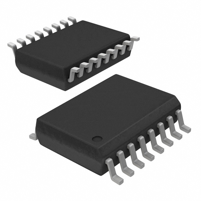
- Part No.:
- DS21600SN
- Manufacturer:
- Analog Devices Inc./Maxim Integrated
- Package:
- 16-SOIC (0.295", 7.50mm Width)
- Datasheet:
-
 DS21600SN.pdf
- Description:
- IC CLOCK RATE ADAPTER 16SOIC
- Quantity:
- Payment:

- Shipping:

Inventory:871
Please send an inquiry. Send us your inquiry, and we will respond immediately.
Product details
Overview
DS21600SN from Maxim Integrated is a 3.3V/5V multiple-rate clock rate adapter IC for E-carrier/T-carrier synchronization, supporting bidirectional 1.544 MHz ↔ 2.048 MHz conversion with frequency-locked CLKOUT1 and CLKOUT2 outputs plus an 8 kHz frame-sync output. It operates across -40°C to +85°C and serves as a direct drop-in replacement for LXP600ASE in telecom line interface units.
For engineers reviewing the DS21600SN datasheet, DS21600SN pinout, DS21600SN application, or DS21600SN equivalent, this device delivers low-jitter, phase-alignable T1/E1 clock translation with no external components required - critical for legacy carrier equipment upgrades and mixed-voltage timing subsystems.
Technical Context
The DS21600SN implements a PLL-based analog clock synthesis architecture with feedback divider and frame-sync generator, enabling precise frequency locking of both CLKOUT1 (T1/E1 rate) and CLKOUT2 (higher multiple rate) to CLKIN. Its SEL pin selects between two fixed conversion modes: 1.544 MHz → 2.048 MHz (SEL = 0) or 2.048 MHz → 1.544 MHz (SEL = 1).
All outputs - CLKOUT1, CLKOUT2, and SYNCOUT - are phase-locked to SYNCIN when asserted, with synchronization settling within 50 ms for 8 kHz SYNCIN. Jitter transfer peaks at ~1.6 ns/ns in the 4–8 kHz band, meeting G.823 and TR62411 specifications for telecom-grade timing integrity.
Key Specifications
| Parameter | Value and Actual Design Meaning |
|---|---|
| Supply Voltage | 3.3 V or 5 V ±5% - supports dual-voltage system integration without level-shifting. |
| Input Clock Range | 1.544 MHz or 2.048 MHz - matches standard T1 and E1 reference frequencies. |
| CLKOUT1 Output | 1.544 MHz or 2.048 MHz - selectable via SEL pin; always frequency-locked to CLKIN. |
| CLKOUT2 Output | 6.144 MHz (SEL=0) or 6.176 MHz (SEL=1) - provides higher-rate clock for oversampling or auxiliary timing. |
| SYNCOUT Frequency | 8 kHz - standard frame-sync output, phase-aligned to CLKIN and SYNCIN when active. |
| Output Jitter (G.823) | 0.018 UIP-P typ. (1.544→2.048 MHz) - meets ITU-T jitter compliance for carrier-grade interfaces. |
| Operating Temp | -40°C to +85°C - industrial temperature rating ensures reliability in outdoor telecom cabinets and central office environments. |
Pinout & Package
DS21600SN is housed in a 16-pin SO (Small Outline) package with 1.27 mm pitch, compliant with JEDEC MS-012AB and RoHS requirements.
| Pin/Terminal | Circuit Role | Design Meaning |
|---|---|---|
| CLKIN | Clock Input | Reference input for all synthesized outputs; accepts 1.544 MHz or 2.048 MHz with ±10,000 ppm capture/lock range. |
| CLKOUT1 | Clock Output 1 | T1/E1 rate output (1.544/2.048 MHz), phase-aligned to CLKIN and SYNCIN; drives line interface chips directly. |
| CLKOUT2 | Clock Output 2 | Higher-rate output (6.144/6.176 MHz); used for sampling clocks or auxiliary timing in multi-rate systems. |
| SYNCOUT | Synchronization Output | 8 kHz frame-sync pulse, locked to CLKIN; aligns with T1/E1 framing boundaries for deterministic data alignment. |
| SYNCIN | Synchronization Input | Enables phase-locking of all outputs to external 8 kHz (or integer subrate) signal; tied high/low if unused. |
| SEL | Mode Select Input | Digital control pin selecting conversion direction: SEL = 0 → 1.544→2.048 MHz; SEL = 1 → 2.048→1.544 MHz. |
| VDD | Positive Supply | Accepts 3.3 V or 5 V ±5%; decoupling required per layout guidelines for low-jitter performance. |
| VSS | Ground | Dedicated ground return; must be connected to clean system ground plane to minimize jitter coupling. |
Key Features
| Feature | Design Value |
|---|---|
| Direct LXP600ASE replacement | Pin-compatible and functionally identical to LXP600ASE, enabling drop-in upgrade of legacy carrier timing modules. |
| Bidirectional E/T-carrier conversion | Supports both 1.544↔2.048 MHz translation paths in one device, eliminating need for separate T1/E1 adapters. |
| No external components | Integrated PLL and dividers eliminate external crystals, capacitors, or loop filters - reduces BOM count and board area. |
| Phase-alignment capability | SYNCIN enables sub-frame synchronization of CLKOUT1, CLKOUT2, and SYNCOUT - essential for TDM multiplexing. |
| Low-jitter output compliance | Meets G.823 and TR62411 jitter specs across full temp range, ensuring interoperability with SONET/SDH and PDH equipment. |
Applications
| Telecom Line Interface Unit (LIU) | T1/E1 Multiplexer Timing |
|---|---|
|
Use Scenario: Interfacing T1 and E1 line cards in hybrid carrier networks where legacy E1 equipment connects to T1 infrastructure. IC Role / Device Role / Timing Role: Clock rate adapter translating between 2.048 MHz E1 and 1.544 MHz T1 reference clocks while maintaining frame alignment. Use Value: Enables seamless interworking without clock domain crossing errors or buffer overflow in framer ASICs. |
Use Scenario: Providing synchronized clocks to multiple TDM channels in a 32-channel E1 multiplexer with embedded T1 tributaries. IC Role / Device Role / Timing Role: Generating CLKOUT1 (1.544 MHz) for T1 channel timing and CLKOUT2 (6.176 MHz) for oversampled data recovery. Use Value: Eliminates need for separate clock synthesizers per tributary, reducing component count and jitter accumulation across channels. |
| Legacy Carrier Equipment Upgrade | PDH Network Synchronization Hub |
|
Use Scenario: Replacing obsolete LXP600ASE in installed base of digital cross-connect systems (DCS) requiring RoHS-compliant parts. IC Role / Device Role / Timing Role: Pin-identical timing adapter preserving existing PCB layout while adding 3.3 V support and improved jitter performance. Use Value: Extends product lifecycle without redesign; avoids costly requalification of timing subsystems. |
Use Scenario: Centralized clock distribution in a regional PDH hub aggregating T1 and E1 feeds from multiple remote sites. IC Role / Device Role / Timing Role: Accepting diverse input clocks (1.544/2.048 MHz) and generating aligned 8 kHz SYNCOUT for frame boundary coordination. Use Value: Ensures deterministic phase relationship across all aggregated streams, preventing slip events in concatenated payloads. |
Equivalent & Alternatives
The following parts are listed as comparable options for similar clock rate adapter applications.
| Alternative Part | Technical Difference | Application Difference | Selection Advice |
|---|---|---|---|
| LXP600ASE | Same pinout and function; older Maxim part with identical AC/DC specs but no lead-free option. | Identical use in legacy LIUs; lacks RoHS compliance and 3.3 V optimization of DS21600SN. | Select LXP600ASE only for exact form-fit-function replacement where RoHS is not mandated. |
| DS21602SN | Supports 1.544→2.048 MHz and 1.544→8.192 MHz conversions; same package and supply but different CLKOUT2 frequency. | Used where 8.192 MHz auxiliary clock is needed (e.g., for 4×T1 framing), not for standard T1/E1 translation. | Choose DS21602SN only if 8.192 MHz output is required; otherwise DS21600SN is optimal for core T1/E1 rate matching. |
Compared with LXP600ASE and DS21602SN, the DS21600SN offers RoHS compliance, guaranteed 3.3 V operation, and optimized jitter performance for standard 1.544/2.048 MHz bidirectional conversion - making it the preferred choice for new designs and upgrades targeting industrial temperature stability and dual-supply flexibility.
Availability
DS21600SN is available at Aetrix Electronics and suitable for telecom line interface units, T1/E1 multiplexers, legacy carrier equipment upgrades, and PDH network synchronization hubs requiring stable component supply across extended temperature ranges.
Supply support for DS21600SN includes scheduled delivery planning, volume procurement assistance, BOM continuity management, traceable sourcing, and lifecycle availability coordination for OEM customers, industrial embedded developers, connected-device designers, and electronics production programs.
Manufacturer
Maxim Integrated (now part of Analog Devices) is a semiconductor company specializing in precision analog, mixed-signal, and power management ICs for industrial, communications, and computing applications.
The DS21600SN belongs to Maxim's legacy telecom timing portfolio, designed specifically to replace obsolete LXP-series clock adapters in E-carrier and T-carrier infrastructure with enhanced voltage flexibility and jitter performance.
FAQ
What is the primary clock conversion function of the DS21600SN?
The DS21600SN performs bidirectional clock rate adaptation between T-carrier (1.544 MHz) and E-carrier (2.048 MHz) standards. When SEL = 0, it converts 1.544 MHz CLKIN to 2.048 MHz CLKOUT1 and 6.144 MHz CLKOUT2; when SEL = 1, it converts 2.048 MHz CLKIN to 1.544 MHz CLKOUT1 and 6.176 MHz CLKOUT2. The DS21600SN maintains strict frequency locking and phase alignment across all outputs.
Does the DS21600SN support both 3.3 V and 5 V operation?
Yes, the DS21600SN operates from either a 3.3 V or 5 V supply, with specified tolerance of ±5% for both voltages. This dual-supply capability allows direct integration into mixed-voltage telecom systems without level shifters. The DS21600SN's internal circuitry is optimized for stable performance across both rails, including jitter and timing parameters.
How does the SYNCIN pin affect timing behavior in the DS21600SN?
The SYNCIN pin enables phase alignment of CLKOUT1, CLKOUT2, and SYNCOUT to an external 8 kHz (or integer subrate) reference. When asserted, the DS21600SN achieves synchronization within 50 ms. If unused, SYNCIN must be tied high or low to prevent floating inputs. This feature ensures deterministic frame boundary alignment in TDM systems - a critical requirement not provided by basic clock dividers.
Is the DS21600SN pin-compatible with the LXP600ASE?
Yes, the DS21600SN is a direct drop-in replacement for the LXP600ASE, with identical pin configuration, electrical characteristics, and functional behavior. The DS21600SN retains full compatibility while adding RoHS compliance, guaranteed 3.3 V operation, and improved jitter transfer response - making it suitable for both new designs and field upgrades of legacy LXP600ASE-based equipment.
What jitter specifications does the DS21600SN meet for telecom applications?
The DS21600SN meets ITU-T G.823 and TR62411 jitter standards, with typical peak-to-peak jitter of 0.018 UI for 1.544→2.048 MHz conversion and 0.025 UI for 2.048→1.544 MHz conversion under specified bandwidth conditions. These values ensure interoperability with SONET/SDH framer ICs and PDH equipment requiring strict jitter compliance - a key validation point for the DS21600SN in carrier-grade deployments.
DS21600SN Specifications
- Product attributes
- Attribute value
- Manufacturer:
- Analog Devices Inc./Maxim Integrated
- Series:
- -
- Package/Case:
- 16-SOIC (0.295", 7.50mm Width)
- Packaging:
- Tube
- Product Status:
- Obsolete
- Programmable:
- Not Verified
- Type:
- Clock Rate Adapter
- PLL:
- Yes
- Input:
- Clock
- Output:
- Clock
- Number of Circuits:
- 1
- Ratio - Input:Output:
- 1:2
- Differential - Input:Output:
- No/No
- Frequency - Max:
- 6.176MHz
- Divider/Multiplier:
- Yes/No
- Voltage - Supply:
- 3.135V ~ 5.25V
- Operating Temperature:
- -40°C ~ 85°C
- Mounting Type:
- Surface Mount
- Grade:
- -
- Qualification:
- -
- Supplier Device Package:
- 16-SOIC
DS21600SN FAQ
1.How can I place an order for DS21600SN through Aetrix?
Please submit a Request for Quotation (RFQ) for DS21600SN on Aetrix. Our sales agent will provide a competitive quotation and guide you through the order confirmation once you accept the terms.
2.Are the price and stock information for DS21600SN reliable?
The price and inventory of DS21600SN are updated periodically and may fluctuate due to market conditions. Stock and pricing data are typically refreshed every 24 hours. Quotation validity for DS21600SN is usually 5 days.
3.What payment methods are accepted for DS21600SN?
We accept Wire Transfer, PayPal, Credit Card, Western Union, MoneyGram, and Escrow for DS21600SN transactions.
Note: Certain payment methods may incur a processing fee.
4.How is shipping managed for DS21600SN?
DS21600SN orders can be shipped via leading logistics carriers, including DHL, UPS, FedEx, TNT, or Registered Mail.
Once your DS21600SN order is processed, you will receive an email with the shipment details and tracking number.
Note: Tracking information may take up to 24 hours to appear. Express delivery typically takes 3–5 business days.
5.How can I obtain technical support or documentation for DS21600SN?
For technical support, including DS21600SN datasheets, pinout diagrams, or application guidance, please contact our engineering support team. They can provide detailed documentation and assistance for your DS21600SN requirements.
6.How does Aetrix verify that DS21600SN is sourced from the original manufacturer or authorized distributors?
All DS21600SN products on Aetrix are procured from qualified distributors and authorized channels. Our dedicated quality assurance team conducts strict verification, including traceability checks and, if necessary, third-party testing. This ensures that DS21600SN meets industry standards.
7.What is the process for return or replacement of DS21600SN?
All DS21600SN units undergo pre-shipment inspection (PSI). If there is an issue with DS21600SN, returns or replacements are accepted under the following conditions:
1.Quantity discrepancies, incorrect items, or visible external defects (such as breakage or corrosion), acknowledged by Aetrix.
2.The issue is reported within 90 days of delivery.
3.The DS21600SN part is unused and in its original packaging.
Return procedure for DS21600SN:
1.Submit a request within 90 days.
2.Obtain a Return Material Authorization (RMA) from Aetrix.
DS21600SN Tags

-
CD74HCT4046AM96
Texas Instruments

-
MC14046BDWR2G
onsemi

-
501MILFT
Renesas
-
CD74HC7046AM
Texas Instruments

-
CDCVF2505PWR
Texas Instruments

-
RC19004A100GNL#KB0
Renesas

-
SI5351A-B-GTR
Skyworks Solutions Inc.

-
CY2305SXI-1T
Infineon Technologies
-
570BILFT
Renesas

-
CDCE913PWR
Texas Instruments
-
CY2305SXI-1HT
Infineon Technologies

-
DS1086LU+T
Analog Devices Inc./Maxim Integrated
Tech Hub

A practical engineering guide to 3.3V and 5V logic compatibility, input thresholds, resistor dividers, translator ICs, MOSFET level shifting, I2C pull-ups, timing limits and power-sequencing risks.

The 74HC595 uses push-pull logic outputs, while the TPIC6B595 uses 50 V open-drain DMOS sinks for higher-power loads. This guide compares timing, current limits, 3.3 V interfacing, load wiring, thermal…

The 74HC595 converts serial data into eight stable parallel outputs. This guide covers pin functions, shift and storage timing, OE and MR behavior, drive-current limits, cascading, voltage compatibilit…

A technical comparison of level-sensitive latches and edge-triggered flip-flops, covering timing windows, setup and hold limits, master–slave operation, time borrowing, race-through, HDL inference and…

A D latch stores one bit while Enable controls when data can pass. This reference covers gate-level operation, truth tables, transparency, setup and hold timing, LE versus OE, common ICs and practical …

An SR latch stores one bit through cross-coupled feedback. This engineering reference covers NOR and NAND implementations, truth tables, forbidden-state recovery, gated operation, switch debouncing, fa…

Latch circuits retain one bit through feedback. This technical reference covers SR and D latches, truth tables, transparency, timing limits, latch-versus-flip-flop behavior, applications and common log…

An engineering guide to LED driver operation, constant-current and constant-voltage outputs, linear and switching topologies, dimming, IC selection, calculations, replacement compatibility, and fault c…

Operational amplifier guide covering op amp basics, feedback, ideal vs real op amps, common configurations, buffer circuits, offset, bias current, gain-bandwidth, slew rate, rail-to-rail limits and sel…

Jumper cables guide covering safe connection order, red and black clamp placement, final ground connection, cable gauge, length, clamp quality, copper vs CCA cables, jump starter comparison and battery…


