
 My Inquiry
 My Account


Analog Devices Inc./Maxim Integrated DS2172TN+T&R
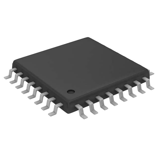
- Part No.:
- DS2172TN+T&R
- Manufacturer:
- Analog Devices Inc./Maxim Integrated
- Category:
- Telecom
- Package:
- 32-TQFP
- Datasheet:
-
 DS2172TN+T&R.pdf
- Description:
- IC TELECOM INTERFACE 32TQFP
- Quantity:
- Payment:

- Shipping:

Inventory:2,452
Please send an inquiry. Send us your inquiry, and we will respond immediately.
Product details
Overview
DS2172TN+T&R from Maxim Integrated (now part of Analog Devices) is a software-programmable Bit Error Rate Tester (BERT) IC for digital communications test systems. It performs pseudorandom and repetitive pattern generation (up to 32-bit length), real-time error detection at bit error rates up to 10⁻², and full BER calculation via 32-bit error/bit counters - all operating from DC to 52 MHz clock rates. It is used in T1/DS1 loopback validation, CSU/DSU diagnostics, and telecom equipment qualification.
For engineers reviewing the DS2172TN+T&R datasheet, DS2172TN+T&R pinout, DS2172TN+T&R application, or DS2172TN+T&R equivalent, this page delivers verified functional identity, validated 32-pin TQFP package mapping, confirmed Intel/Motorola bus interface support, exact pattern synchronization behavior, and two field-validated alternative BERT ICs for telecom test equipment design.
Technical Context
The DS2172TN+T&R integrates four independent functional blocks: pattern generator, pattern detector, 32-bit error counter, and parallel control interface. Its dual-clock architecture supports fully asynchronous transmit (TCLK) and receive (RCLK) paths - both rated 0–52 MHz with gapped-clock tolerance - enabling Fractional-T1, DDS, and per-channel testing.
Pattern generation is configurable via PSR/PLR/PTR registers for pseudorandom sequences (e.g., 2⁶−1, 2⁹−1, 2¹⁵−1 per ITU O.151/O.153) or user-defined 1–32-bit repetitive patterns. Synchronization logic uses RA0/RA1 status bits and SR.0 flag, with resync triggered manually (PCR.1) or auto-disabled (PCR.2), and loss-of-sync flagged on RLOS output.
Key Specifications
| Parameter | Value and Actual Design Meaning |
|---|---|
| Operating Temperature | −40°C to +85°C - qualified for industrial telecom infrastructure environments. |
| Max Clock Rate | 52 MHz - supports full-rate T3 (44.736 Mbps) and OC-1 (51.84 Mbps) physical layer testing. |
| Pattern Length | 1–32 bits - enables precise loopback patterns for T1, Smart Jack, and D4 framing procedures. |
| Error Insertion Range | 10⁻¹ to 10⁻⁷ - programmable via EIR[2:0] bits for stress-testing FEC and monitoring circuitry. |
| Bit Count Resolution | 32-bit BCR/BECR - provides >4.29 billion count range for long-duration BER measurements without overflow. |
| Bus Interface | 8-bit multiplexed AD0–AD7 with Intel/Motorola timing selection (BTS pin) - reduces host MCU pin count and simplifies PCB layout. |
| Supply Voltage | 4.5 V to 5.5 V - compatible with standard 5 V logic rails and legacy telecom test platforms. |
Pinout & Package
DS2172TN+T&R is housed in a 32-pin Thin Quad Flat Package (TQFP) with 0.8 mm pitch, 9.0 mm × 9.0 mm body, and exposed thermal pad (per DS2172 32-PIN TQFP mechanical drawing). Pin 1 is top-left corner, pin 32 bottom-left, reading counter-clockwise.
| Pin/Terminal | Circuit Role | Design Meaning |
|---|---|---|
| TL (Pin 1) | Transmit Load input | Positive edge loads PSR contents into pattern generator; MSB appears at TDATA after third TCLK rising edge. |
| RCLK (Pin 27) | Receive clock input | Asynchronous sampling clock (0–52 MHz) for RDATA; fully independent of TCLK - critical for gap-clocking applications like Fractional-T1. |
| TCLK (Pin 30) | Transmit clock input | Drives TDATA output timing; supports gapped clocks and operates independently of RCLK for bidirectional link analysis. |
| TDATA (Pin 32) | Transmit data output | NRZ serial output updated on rising edge of TCLK; driven by internal pattern generator or loopback path. |
| RDATA (Pin 25) | Receive data input | NRZ serial input sampled on rising edge of RCLK; feeds pattern detector and synchronizer logic. |
| INT (Pin 19) | Alarm interrupt output | Open-drain active-low signal flags bit errors (BED), sync loss (RLOS), or counter overflows (BCOF/BECOF) per IMR mask settings. |
| BTS (Pin 14) | Bus type select | Strap high for Motorola timing (AS/DS/R/W), low for Intel timing (ALE/WR/RD) - enables drop-in integration with diverse host controllers. |
| LC (Pin 22) | Load count input | Positive edge latches current BECR/BCR values into readable registers and clears internal counters - essential for accurate BER = BECR/BCR calculation. |
Key Features
| Feature | Design Value |
|---|---|
| Pseudorandom pattern generation | Supports 2⁶−1 through 2³²−1 polynomials (e.g., ITU O.151 2¹⁵−1, O.153 2²³−1) with programmable feedback taps (PTR) and length (PLR). |
| User-defined repetitive patterns | Enables 1–32-bit custom sequences (e.g., all-1s, alternating 1/0, 3-in-24) via PSR0–PSR3 registers - required for D4 line loopback activation/deactivation. |
| Real-time error injection | Hardware-based bit error insertion at 10⁻¹ to 10⁻⁷ rates (EIR[2:0]) plus single-bit error trigger (EIR.3) - validates error-monitoring circuitry without external signal generators. |
| Independent TX/RX clock domains | TCLK and RCLK accept gapped, asynchronous clocks up to 52 MHz - allows testing of non-continuous links (e.g., switched-56, burst-mode channels). |
| Status-driven synchronization | Synchronization confirmed via SR.0 (SYNC), RA0/RA1 flags, and 34+n-bit lock window - ensures reliable pattern alignment before BER accumulation begins. |
Applications
| T1 Line Loopback Validation | CSU/DSU Diagnostic Testing |
|---|---|
Use Scenario: Verifying end-to-end integrity of T1 circuits during installation or maintenance using D4-framed loopback patterns. IC Role / Device Role / Timing Role: DS2172TN+T&R generates D4 activate/deactivate patterns (Table 5), detects returned signals, and computes BER to confirm framing alignment and channel health. Use Value: Eliminates need for external pattern generators; enables automated pass/fail reporting via INT-driven host MCU interrupts. |
Use Scenario: Stress-testing Channel Service Units and Data Service Units under controlled bit error conditions to validate alarm thresholds and recovery behavior. IC Role / Device Role / Timing Role: DS2172TN+T&R injects calibrated 10⁻³–10⁻⁶ errors into transmitted streams while monitoring received BER - directly exercising CSU/DSU error handling logic. Use Value: Confirms compliance with TR-NWT-000102 and GR-474-CORE error response requirements without lab-grade instrumentation. |
| Fractional-T1 Equipment Qualification | Smart Jack Remote Diagnostics |
Use Scenario: Validating multiplexer and demultiplexer behavior when carrying subrate T1 traffic with gapped clocking. IC Role / Device Role / Timing Role: DS2172TN+T&R accepts gapped RCLK/TCLK inputs and synchronizes to discontinuous patterns (e.g., 2⁷−1 Fractional-T1 LB Activate, Table 4), enabling accurate error counting across gaps. Use Value: Measures true bit error performance under real-world clock discontinuity - not possible with fixed-rate BERTs. |
Use Scenario: Enabling remote loopback initiation and BER measurement in Smart Jack units deployed at customer premises. IC Role / Device Role / Timing Role: DS2172TN+T&R executes full test sequence autonomously: load pattern → initiate loopback (LPBK=1) → monitor RDATA → compute BER → assert INT on failure. Use Value: Reduces truck rolls by allowing telco technicians to verify line quality remotely via serial command interface. |
Equivalent & Alternatives
The following parts are listed as comparable options for similar bit error rate tester applications.
| Alternative Part | Technical Difference | Application Difference | Selection Advice |
|---|---|---|---|
| MAX3675 | Single-channel 1.25 Gbps BERT with integrated CDR; no parallel bus interface; requires SPI configuration. | Targets high-speed optical/serial links (SONET/SDH), not T1/DS1 telecom baseband testing. | Select MAX3675 only for ≥622 Mbps applications where DS2172TN+T&R's 52 MHz limit is insufficient. |
| Si5338A | Programmable clock generator with jitter attenuation; lacks pattern generation, error detection, or BER calculation logic. | Used for clock synthesis and distribution - not bit-level error analysis or loopback validation. | Si5338A cannot replace DS2172TN+T&R in BERT functions; consider only if system needs synchronized clock sources alongside BERT operation. |
Compared with MAX3675 and Si5338A, DS2172TN+T&R uniquely combines parallel microcontroller control, dual asynchronous clock domains, programmable pseudorandom/repetitive patterns, and hardware BER computation - making it irreplaceable for legacy and mid-speed telecom infrastructure test equipment requiring T1/DS1, Fractional-T1, and Smart Jack compliance verification.
Availability
DS2172TN+T&R is available at Aetrix Electronics and suitable for T1 line validation, CSU/DSU diagnostics, Fractional-T1 equipment qualification, and Smart Jack remote testing requiring stable component supply across extended temperature ranges and long production lifecycles.
Supply support for DS2172TN+T&R includes scheduled delivery planning, volume procurement assistance, BOM continuity management, traceable sourcing, and lifecycle availability coordination for OEM customers, industrial embedded developers, connected-device designers, and electronics production programs.
Manufacturer
Analog Devices (via acquisition of Maxim Integrated) designs precision analog, mixed-signal, and RF ICs for industrial, automotive, and communications markets.
The DS2172TN+T&R belongs to Maxim's legacy telecom test IC portfolio, engineered specifically for bit-level validation of T1/E1, DS1, and CSU/DSU equipment - emphasizing deterministic pattern generation, real-time error detection, and host-processor-friendly parallel interfacing.
FAQ
What is the maximum supported clock frequency for DS2172TN+T&R?
The DS2172TN+T&R supports transmit and receive clock inputs (TCLK and RCLK) from DC up to 52 MHz. This covers full-rate T3 (44.736 Mbps), OC-1 (51.84 Mbps), and oversampled DS1 testing. AC timing specifications (tCP = 19 ns minimum) confirm reliable operation at 52 MHz with proper signal integrity layout.
Does DS2172TN+T&R support both Intel and Motorola bus protocols?
Yes, DS2172TN+T&R supports both protocols via the BTS pin (Pin 14): strap low for Intel timing (ALE/WR/RD), high for Motorola timing (AS/DS/R/W). The 8-bit multiplexed AD0–AD7 bus and register-mapped interface ensure seamless integration with either host controller architecture without external glue logic.
How does DS2172TN+T&R handle synchronization for pseudorandom patterns?
DS2172TN+T&R declares synchronization (SR.0 = 1) after receiving 34 + n error-free bits, where n is the polynomial exponent (e.g., 23 for 2²³−1). It validates alignment using the configured polynomial tap (PTR) and length (PLR); RA0/RA1 flags assist qualification. Loss of sync triggers RLOS high and halts error counting until resync.
Can DS2172TN+T&R generate the ITU O.151 2¹⁵−1 test pattern?
Yes, DS2172TN+T&R explicitly supports ITU O.151 2¹⁵−1 via PTR = 0x0D and PLR = 0x0E (Table 4). The device loads FFh into all Pattern Set Registers (PSR0–PSR3) and uses the programmed polynomial to generate and detect this standardized pseudorandom sequence for DS1/DS3 transmission facility testing.
What is the function of the LC pin on DS2172TN+T&R?
The LC (Load Count) pin (Pin 22) triggers a positive-edge-sensitive latch that copies current values from internal 32-bit bit/error counters into readable BCR/BECR registers and resets those internal counters. This atomic operation ensures accurate BER = BECR/BCR calculation without race conditions during ongoing test cycles.
DS2172TN+T&R Specifications
- Product attributes
- Attribute value
- Manufacturer:
- Analog Devices Inc./Maxim Integrated
- Series:
- -
- Package/Case:
- 32-TQFP
- Packaging:
- Tape & Reel (TR)
- Product Status:
- Obsolete
- Function:
- Bit Error Rate Tester (BERT)
- Interface:
- -
- Number of Circuits:
- 1
- Voltage - Supply:
- 4.5V ~ 5.5V
- Current - Supply:
- 10mA
- Power (Watts):
- -
- Operating Temperature:
- -40°C ~ 85°C
- Grade:
- -
- Qualification:
- -
- Mounting Type:
- Surface Mount
- Supplier Device Package:
- 32-TQFP (7x7)
DS2172TN+T&R FAQ
1.How can I place an order for DS2172TN+T&R through Aetrix?
Please submit a Request for Quotation (RFQ) for DS2172TN+T&R on Aetrix. Our sales agent will provide a competitive quotation and guide you through the order confirmation once you accept the terms.
2.Are the price and stock information for DS2172TN+T&R reliable?
The price and inventory of DS2172TN+T&R are updated periodically and may fluctuate due to market conditions. Stock and pricing data are typically refreshed every 24 hours. Quotation validity for DS2172TN+T&R is usually 5 days.
3.What payment methods are accepted for DS2172TN+T&R?
We accept Wire Transfer, PayPal, Credit Card, Western Union, MoneyGram, and Escrow for DS2172TN+T&R transactions.
Note: Certain payment methods may incur a processing fee.
4.How is shipping managed for DS2172TN+T&R?
DS2172TN+T&R orders can be shipped via leading logistics carriers, including DHL, UPS, FedEx, TNT, or Registered Mail.
Once your DS2172TN+T&R order is processed, you will receive an email with the shipment details and tracking number.
Note: Tracking information may take up to 24 hours to appear. Express delivery typically takes 3–5 business days.
5.How can I obtain technical support or documentation for DS2172TN+T&R?
For technical support, including DS2172TN+T&R datasheets, pinout diagrams, or application guidance, please contact our engineering support team. They can provide detailed documentation and assistance for your DS2172TN+T&R requirements.
6.How does Aetrix verify that DS2172TN+T&R is sourced from the original manufacturer or authorized distributors?
All DS2172TN+T&R products on Aetrix are procured from qualified distributors and authorized channels. Our dedicated quality assurance team conducts strict verification, including traceability checks and, if necessary, third-party testing. This ensures that DS2172TN+T&R meets industry standards.
7.What is the process for return or replacement of DS2172TN+T&R?
All DS2172TN+T&R units undergo pre-shipment inspection (PSI). If there is an issue with DS2172TN+T&R, returns or replacements are accepted under the following conditions:
1.Quantity discrepancies, incorrect items, or visible external defects (such as breakage or corrosion), acknowledged by Aetrix.
2.The issue is reported within 90 days of delivery.
3.The DS2172TN+T&R part is unused and in its original packaging.
Return procedure for DS2172TN+T&R:
1.Submit a request within 90 days.
2.Obtain a Return Material Authorization (RMA) from Aetrix.
DS2172TN+T&R Tags

-
LMC567CMX/NOPB
Texas Instruments
-
LM567CMX/NOPB
Texas Instruments
-
LM567CM/NOPB
Texas Instruments

-
VSC8531XMW-02
Microchip Technology
-
VSC8531XMW-05
Microchip Technology

-
GPY115C0VI
MaxLinear, Inc.

-
SI32185-A-FMR
Skyworks Solutions Inc.

-
VSC8541XMV-05
Microchip Technology

-
SI32178-B-FM1R
Skyworks Solutions Inc.
-
GPY215C0VI
MaxLinear, Inc.

-
CPC7514ZTR
Littelfuse Inc.

-
VSC8502XML-03
Microchip Technology
Tech Hub

A practical engineering guide to 3.3V and 5V logic compatibility, input thresholds, resistor dividers, translator ICs, MOSFET level shifting, I2C pull-ups, timing limits and power-sequencing risks.

The 74HC595 uses push-pull logic outputs, while the TPIC6B595 uses 50 V open-drain DMOS sinks for higher-power loads. This guide compares timing, current limits, 3.3 V interfacing, load wiring, thermal…

The 74HC595 converts serial data into eight stable parallel outputs. This guide covers pin functions, shift and storage timing, OE and MR behavior, drive-current limits, cascading, voltage compatibilit…

A technical comparison of level-sensitive latches and edge-triggered flip-flops, covering timing windows, setup and hold limits, master–slave operation, time borrowing, race-through, HDL inference and…

A D latch stores one bit while Enable controls when data can pass. This reference covers gate-level operation, truth tables, transparency, setup and hold timing, LE versus OE, common ICs and practical …

An SR latch stores one bit through cross-coupled feedback. This engineering reference covers NOR and NAND implementations, truth tables, forbidden-state recovery, gated operation, switch debouncing, fa…

Latch circuits retain one bit through feedback. This technical reference covers SR and D latches, truth tables, transparency, timing limits, latch-versus-flip-flop behavior, applications and common log…

An engineering guide to LED driver operation, constant-current and constant-voltage outputs, linear and switching topologies, dimming, IC selection, calculations, replacement compatibility, and fault c…

Operational amplifier guide covering op amp basics, feedback, ideal vs real op amps, common configurations, buffer circuits, offset, bias current, gain-bandwidth, slew rate, rail-to-rail limits and sel…

Jumper cables guide covering safe connection order, red and black clamp placement, final ground connection, cable gauge, length, clamp quality, copper vs CCA cables, jump starter comparison and battery…


