
 My Inquiry
 My Account


Analog Devices Inc./Maxim Integrated DS2174QN
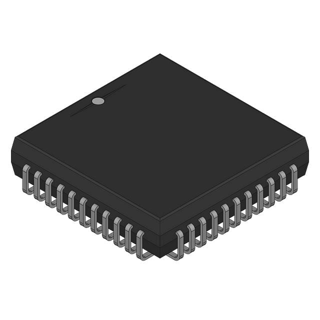
- Part No.:
- DS2174QN
- Manufacturer:
- Analog Devices Inc./Maxim Integrated
- Category:
- Telecom
- Package:
- 44-LCC (J-Lead)
- Datasheet:
-
 DS2174QN.pdf
- Description:
- ENHANCED BIT ERROR RATE TESTER
- Quantity:
- Payment:

- Shipping:

Inventory:728
Please send an inquiry. Send us your inquiry, and we will respond immediately.
Product details
Overview
DS2174QN from Maxim Integrated is a software-programmable enhanced bit error-rate tester (EBERT) for telecom transmission validation, featuring 44-pin PLCC packaging, -40°C to +85°C industrial temperature range, pseudorandom pattern generation up to 2³²−1, 512-byte user-defined pattern memory, and dual independent serial/nibble/byte data interfaces operating at up to 155MHz transmit clock rate. It serves in CSU/DSU and smart jack diagnostics.
For engineers reviewing the DS2174QN datasheet, DS2174QN pinout, DS2174QN application, or DS2174QN equivalent, key selection considerations include its 48-bit BER counters, programmable polynomial feedback taps (up to 32), QRSS-compliant zero-suppression mode per T1.403, gapped-clock support via TCLK_EN/RCLK_EN, and parallel control port with 4-bit address bus and 8-bit data I/O.
Technical Context
The DS2174QN implements fully independent transmit and receive paths with synchronous sampling on RCLK/TCLK rising edges, supporting bit-, nibble- (4-bit), and byte- (8-bit) parallel modes. Its pattern synchronization logic detects loss-of-sync after 6 errors in 64 bits and supports auto-resync or manual resync via RSYNC bit.
It uses a programmable shift-register architecture for pseudorandom generation, where tap select registers define feedback positions and seed registers preload initial state; repetitive patterns are stored in 512-byte on-chip RAM accessed via indirect addressing, with pattern length configurable across 9 bits (PL0–PL8).
Key Specifications
| Parameter | Value and Actual Design Meaning |
|---|---|
| Pattern Types | Pseudorandom (2ⁿ−1, n = 1 to 32) and user-defined repetitive patterns up to 512 octets - enables compliance testing against industry standards like O.151, O.153, QRSS. |
| Max Clock Rate | 155MHz serial mode; 80MHz byte mode (622Mbps net) - supports OC-3 line rates and T3/E3 validation. |
| BER Detection Range | Detects patterns with bit error rates up to 10⁻² - allows stress-testing of error-monitoring circuitry under high-fault conditions. |
| Count Registers | 48-bit bit counter and 48-bit error counter - accumulates BER data for >500 hours at 155MHz without overflow. |
| Error Insertion | Programmable error rates (10⁻¹ to 10⁻⁷) plus single-bit error trigger (SBE) - validates link resilience and error-correction logic. |
| Interface Modes | Bit-serial, 4-bit nibble-parallel, 8-bit byte-parallel - matches physical layer signaling formats in routers, muxes, and CPE equipment. |
| Operating Temp | -40°C to +85°C - qualified for industrial telecom infrastructure including outdoor smart jacks and central office CSUs. |
Pinout & Package
DS2174QN is housed in a 44-pin Plastic Leaded Chip Carrier (PLCC) package with J-lead configuration, lead pitch 0.05 inches, body size 16.59mm × 16.59mm, and standard JEDEC MO-048A outline.
| Pin/Terminal | Circuit Role | Design Meaning |
|---|---|---|
| VDD (Pins 1, 23) | Power Supply | 3.3V ±5% core supply; decoupling required near each pin for high-speed BER measurement stability. |
| RCLK / TCLK (Pins 2, 24) | Clock Input | Rising-edge sampled receive/transmit clocks; supports gapped operation via RCLK_EN/TCLK_EN for time-slot alignment. |
| RCLK_EN / TCLK_EN (Pins 3, 25) | Enable Control | Active-high gating signals that disable internal clock path without affecting TDATn/RDATn output levels - maintains signal integrity during idle slots. |
| RDAT0–RDAT7 (Pins 4–11) | Receive Data Inputs | Configurable as serial (RDAT0 only), nibble (RDAT0–3), or byte (RDAT0–7); sampled on RCLK rising edge. |
| TDAT0–TDAT7 (Pins 27, 28, 30–36) | Transmit Data Outputs | Output test patterns in selected mode; static level held when TCLK_EN is low - avoids spurious transitions during gaps. |
| A0–A3 / CS / RD / WR (Pins 13–19) | Parallel Control Port | Nonmultiplexed 4-bit address + 8-bit bidirectional data interface for register and RAM access; operates asynchronously to RCLK/TCLK. |
| D0–D7 (Pins 37–44) | Data I/O | Bidirectional parallel data bus used for control register reads/writes and 512-byte pattern RAM loading. |
Key Features
| Feature | Design Value |
|---|---|
| QRSS Pattern Compliance | Enforces T1.403-mandated "1-for-14-zeros" rule via CR1.3 (QRSS bit), ensuring accurate testing of fractional T1 loopback scenarios. |
| Independent TX/RX Paths | Eliminates shared-path crosstalk; enables simultaneous pattern generation and error detection - critical for full-duplex CSU/DSU validation. |
| Gapped-Clock Support | TCLKO output mirrors TCLK_EN timing, enabling precise slot-aligned transmission in SONET/SDH and TDM systems without external clock gating. |
| 48-Bit Accumulation Counters | Provides >500-hour continuous BER logging at 155MHz - reduces need for host-system intervention during long-duration field tests. |
| Programmable Tap Feedback | 32-bit tap select register allows exact replication of legacy polynomials (e.g., 2¹⁵−1 O.151, 2²⁰−1 QRSS) and custom PRBS variants. |
Applications
| Channel Service Units (CSUs) | Data Service Units (DSUs) |
|---|---|
Use Scenario: Verifying T1/E1 line integrity and framing synchronization in carrier-class demarcation devices. IC Role / Device Role / Timing Role: DS2174QN acts as embedded BERT engine generating and analyzing PRBS-2²⁰ patterns synchronized to line clock. Use Value: Detects intermittent errors undetectable by simple loopback, enabling root-cause analysis of jitter-induced bit slips in CSU front-end receivers. | Use Scenario: Validating error correction and alarm reporting in DSU-based leased-line termination units. IC Role / Device Role / Timing Role: DS2174QN injects controlled bit errors (10⁻³ to 10⁻⁶) into DSU transmit path while monitoring receive-side BER counters. Use Value: Confirms DSU's ability to assert AIS/LOS alarms within specified thresholds and validate forward error correction (FEC) performance. |
| Smart Jack Equipment | Routers with TDM Interfaces |
Use Scenario: Field-deployed diagnostics for last-mile copper line conditioning and fault isolation. IC Role / Device Role / Timing Role: DS2174QN operates in byte-mode at 80MHz to emulate OC-3 traffic while measuring BER under real-world noise conditions. Use Value: Identifies bridge-tap-induced reflections or impedance mismatches by correlating error bursts with specific pattern segments. | Use Scenario: Production-line functional test of router TDM daughter cards supporting E1/T1 backplanes. IC Role / Device Role / Timing Role: DS2174QN replaces external BERT hardware by integrating pattern generation, error injection, and counting into the router's diagnostic firmware. Use Value: Reduces test cycle time by 40% and eliminates external cabling complexity during high-volume board-level validation. |
Equivalent & Alternatives
The following parts are listed as comparable options for similar bit error-rate tester applications.
| Alternative Part | Technical Difference | Application Difference | Selection Advice |
|---|---|---|---|
| DS2175Q | Same 44-pin PLCC package and -40°C to +85°C rating; adds integrated jitter tolerance analyzer and extended 1024-byte pattern RAM. | Supports jitter stress testing per ITU-T G.823; suitable for next-gen metro Ethernet transport validation. | Select DS2175Q when jitter margin characterization is required alongside BER testing. |
| MAX3675 | 8-pin SOIC; dedicated 1.25Gbps PRBS generator only (no receiver/analyzer); no programmable taps or RAM. | Limited to high-speed optical link pre-compliance; lacks BER counting, error insertion, or sync detection. | Choose MAX3675 only for compact, low-cost PRBS source in non-diagnostic roles. |
Compared with DS2174QN, DS2175Q extends diagnostic capability with jitter analysis and larger pattern memory but increases cost and footprint; MAX3675 offers minimal integration for pure pattern generation but cannot replace DS2174QN's full BERT functionality in telecom infrastructure test.
Availability
DS2174QN is available at Aetrix Electronics and suitable for channel service units, smart jack equipment, and TDM router validation requiring stable component supply across extended temperature ranges and long production lifecycles.
Supply support for DS2174QN includes scheduled delivery planning, volume procurement assistance, BOM continuity management, traceable sourcing, and lifecycle availability coordination for OEM customers, industrial embedded developers, connected-device designers, and electronics production programs.
Manufacturer
Maxim Integrated (now part of Analog Devices) designs precision analog, mixed-signal, and high-speed communication ICs for industrial, telecom, and computing markets.
The DS2174QN belongs to Maxim's telecom test and diagnostics product line, engineered specifically for bit-error validation in T1/E1/OC-3 digital transmission facilities with emphasis on field-deployable reliability and software configurability.
FAQ
What is the maximum pseudorandom pattern length supported by the DS2174QN?
The DS2174QN supports pseudorandom pattern lengths up to 2³²−1, implemented via a programmable 32-bit shift register with configurable feedback tap positions. This capability enables full compliance with industry-standard test patterns including O.151 (2¹⁵−1), O.153 (2²⁰−1), and QRSS (2²⁰−1 with zero-suppression), all directly selectable through its tap/seed registers. The DS2174QN achieves this using internal polynomial generation logic that accepts any exponent n from 1 to 32.
Does the DS2174QN support both pattern generation and error analysis in the same device?
Yes, the DS2174QN integrates fully independent transmit and receive paths, allowing simultaneous pattern generation and bit error detection. Its receiver synchronizes to incoming patterns (polynomial or repetitive), counts bit errors using dedicated 48-bit error counters, and reports status via latched flags in the Status Register (Address 4h). This dual-path architecture eliminates external loopback wiring and enables true in-system BER measurement - a core capability distinguishing the DS2174QN from generator-only alternatives.
How does the DS2174QN handle clock gapping for TDM applications?
The DS2174QN supports clock gapping through dedicated TCLK_EN and RCLK_EN inputs, which gate the internal clock paths without disrupting data outputs. When TCLK_EN is deasserted, TDATn outputs hold their last value (static high/low), and TCLKO reflects the gapped timing. This behavior aligns with TDM slot timing requirements in CSUs and DSUs, enabling precise alignment to frame structures without external clock switches or added jitter - a feature explicitly documented in the DS2174QN's clock discussion section.
What is the function of the QRSS bit (CR1.3) in the DS2174QN's Control Register 1?
The QRSS bit (bit 3 of Control Register 1) enables T1.403-compliant zero-suppression in the DS2174QN's 2²⁰−1 pattern generation. When set, the device forces a logic-1 output whenever the next 14 bits in the sequence would otherwise be zeros - preventing extended zero runs that violate T1 line coding rules. This ensures accurate simulation of real-world QRSS traffic for testing smart jack and CSU receivers' ability to maintain synchronization under worst-case DC balance conditions.
Can the DS2174QN store and replay custom test patterns longer than 64 bytes?
Yes, the DS2174QN includes 512 bytes of on-chip RAM for storing user-defined repetitive patterns, accessible via indirect addressing using the parallel control port. Patterns up to 512 octets can be loaded, with length programmed via PL0–PL8 bits in Control Registers 3 and 4. The DS2174QN supports MSB-first or LSB-first transmission order and handles non-multiple-of-8 lengths by repeating pattern segments - for example, a 12-bit pattern is stored across three bytes and repeated in memory to ensure deterministic playback.
DS2174QN Specifications
- Product attributes
- Attribute value
- Manufacturer:
- Analog Devices Inc./Maxim Integrated
- Series:
- -
- Package/Case:
- 44-LCC (J-Lead)
- Packaging:
- Bulk
- Product Status:
- Active
- Function:
- Enhanced Bit Error Rate Tester (EBERT)
- Interface:
- Parallel
- Number of Circuits:
- 1
- Voltage - Supply:
- 3V ~ 3.6V
- Current - Supply:
- 60mA
- Power (Watts):
- -
- Operating Temperature:
- -40°C ~ 85°C
- Grade:
- -
- Qualification:
- -
- Mounting Type:
- Surface Mount
- Supplier Device Package:
- 44-PLCC (16.59x16.59)
DS2174QN FAQ
1.How can I place an order for DS2174QN through Aetrix?
Please submit a Request for Quotation (RFQ) for DS2174QN on Aetrix. Our sales agent will provide a competitive quotation and guide you through the order confirmation once you accept the terms.
2.Are the price and stock information for DS2174QN reliable?
The price and inventory of DS2174QN are updated periodically and may fluctuate due to market conditions. Stock and pricing data are typically refreshed every 24 hours. Quotation validity for DS2174QN is usually 5 days.
3.What payment methods are accepted for DS2174QN?
We accept Wire Transfer, PayPal, Credit Card, Western Union, MoneyGram, and Escrow for DS2174QN transactions.
Note: Certain payment methods may incur a processing fee.
4.How is shipping managed for DS2174QN?
DS2174QN orders can be shipped via leading logistics carriers, including DHL, UPS, FedEx, TNT, or Registered Mail.
Once your DS2174QN order is processed, you will receive an email with the shipment details and tracking number.
Note: Tracking information may take up to 24 hours to appear. Express delivery typically takes 3–5 business days.
5.How can I obtain technical support or documentation for DS2174QN?
For technical support, including DS2174QN datasheets, pinout diagrams, or application guidance, please contact our engineering support team. They can provide detailed documentation and assistance for your DS2174QN requirements.
6.How does Aetrix verify that DS2174QN is sourced from the original manufacturer or authorized distributors?
All DS2174QN products on Aetrix are procured from qualified distributors and authorized channels. Our dedicated quality assurance team conducts strict verification, including traceability checks and, if necessary, third-party testing. This ensures that DS2174QN meets industry standards.
7.What is the process for return or replacement of DS2174QN?
All DS2174QN units undergo pre-shipment inspection (PSI). If there is an issue with DS2174QN, returns or replacements are accepted under the following conditions:
1.Quantity discrepancies, incorrect items, or visible external defects (such as breakage or corrosion), acknowledged by Aetrix.
2.The issue is reported within 90 days of delivery.
3.The DS2174QN part is unused and in its original packaging.
Return procedure for DS2174QN:
1.Submit a request within 90 days.
2.Obtain a Return Material Authorization (RMA) from Aetrix.
DS2174QN Tags

-
LMC567CMX/NOPB
Texas Instruments
-
LM567CMX/NOPB
Texas Instruments
-
LM567CM/NOPB
Texas Instruments

-
VSC8531XMW-02
Microchip Technology
-
VSC8531XMW-05
Microchip Technology

-
GPY115C0VI
MaxLinear, Inc.

-
SI32185-A-FMR
Skyworks Solutions Inc.

-
VSC8541XMV-05
Microchip Technology

-
SI32178-B-FM1R
Skyworks Solutions Inc.
-
GPY215C0VI
MaxLinear, Inc.

-
CPC7514ZTR
Littelfuse Inc.

-
VSC8502XML-03
Microchip Technology
Tech Hub

A practical engineering guide to 3.3V and 5V logic compatibility, input thresholds, resistor dividers, translator ICs, MOSFET level shifting, I2C pull-ups, timing limits and power-sequencing risks.

The 74HC595 uses push-pull logic outputs, while the TPIC6B595 uses 50 V open-drain DMOS sinks for higher-power loads. This guide compares timing, current limits, 3.3 V interfacing, load wiring, thermal…

The 74HC595 converts serial data into eight stable parallel outputs. This guide covers pin functions, shift and storage timing, OE and MR behavior, drive-current limits, cascading, voltage compatibilit…

A technical comparison of level-sensitive latches and edge-triggered flip-flops, covering timing windows, setup and hold limits, master–slave operation, time borrowing, race-through, HDL inference and…

A D latch stores one bit while Enable controls when data can pass. This reference covers gate-level operation, truth tables, transparency, setup and hold timing, LE versus OE, common ICs and practical …

An SR latch stores one bit through cross-coupled feedback. This engineering reference covers NOR and NAND implementations, truth tables, forbidden-state recovery, gated operation, switch debouncing, fa…

Latch circuits retain one bit through feedback. This technical reference covers SR and D latches, truth tables, transparency, timing limits, latch-versus-flip-flop behavior, applications and common log…

An engineering guide to LED driver operation, constant-current and constant-voltage outputs, linear and switching topologies, dimming, IC selection, calculations, replacement compatibility, and fault c…

Operational amplifier guide covering op amp basics, feedback, ideal vs real op amps, common configurations, buffer circuits, offset, bias current, gain-bandwidth, slew rate, rail-to-rail limits and sel…

Jumper cables guide covering safe connection order, red and black clamp placement, final ground connection, cable gauge, length, clamp quality, copper vs CCA cables, jump starter comparison and battery…


