
 My Inquiry
 My Account


Analog Devices Inc./Maxim Integrated DS2175SN+
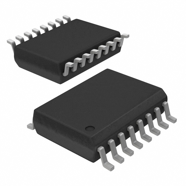
- Part No.:
- DS2175SN+
- Manufacturer:
- Analog Devices Inc./Maxim Integrated
- Category:
- Telecom
- Package:
- 16-SOIC (0.295", 7.50mm Width)
- Datasheet:
-
 DS2175SN+.pdf
- Description:
- IC TELECOM INTERFACE 16SOIC
- Quantity:
- Payment:

- Shipping:

Inventory:1,034
Please send an inquiry. Send us your inquiry, and we will respond immediately.
Product details
Overview
DS2175SN+ from Maxim Integrated (now part of Analog Devices) is a low-power CMOS elastic-store memory IC designed for T1/CEPT rate buffering and synchronization between asynchronous PCM data streams. It supports 1.544 MHz (T1) and 2.048 MHz (CEPT) clock domains, provides 2-frame buffer depth, slip detection and reporting, and operates across industrial temperature range (–40°C to +85°C). It is used in digital cross-connects, PABX-to-computer interfaces, and drop-and-insert equipment.
For engineers reviewing the DS2175SN+ datasheet, DS2175SN+ pinout, DS2175SN+ application, or DS2175SN+ equivalent, key selection considerations include frame-synchronized slip control, dual-rate clock select (RCLKSEL/SCLKSEL), open-collector SLIP output with FSD direction reporting, real-time buffer depth monitoring via RMSYNC/SMSYNC timing, and compatibility with DS2180A/DS2181A transceivers.
Technical Context
The DS2175SN+ implements an elastic store using dual-rate, frame-aligned 2-frame buffering (48 or 64 bytes depending on mode) to synchronize T1 and CEPT data streams without requiring external support logic. Its slip control logic ensures all slips occur strictly on frame boundaries, with ALN-triggered recentering and latched FSD output indicating slip direction (buffer full vs. empty).
It features independent receive (RCLK/RCLKSEL) and system (SYSCLK/SCLKSEL) clock domain selection, serial/parallel backplane support via S/P input, and outputs including SCHCLK (channel clock), SMSYNC (slip-compensated multiframe sync), and SSER (system serial data updated on SYSCLK rising edge).
Key Specifications
| Parameter | Value and Actual Design Meaning |
|---|---|
| Supply Voltage | 4.5 V to 5.5 V - compatible with standard 5 V TTL/CMOS systems; no level-shifting required. |
| Operating Temperature | –40°C to +85°C - qualified for industrial-grade telecom infrastructure deployment. |
| Buffer Depth | 2 frames - provides ≤250 µs total delay while enabling short-term jitter absorption between T1 and CEPT rates. |
| Slip Reporting | SLIP (active-low open-collector) held low for 65 SYSCLK cycles; FSD indicates direction - enables precise fault logging and system-level slip response. |
| Timing Accuracy | tPVD (SYSCLK to SSER) ≤75 ns - ensures deterministic data alignment for high-speed TDM backplanes. |
| Input Compatibility | RCLK/RMSYNC/SFSYNC/ALN setup/hold ≥20 ns - supports robust interface timing with standard ECL/TTL clock sources. |
| Power Consumption | ID D = 9–16 mA at 5 V - low static power ideal for dense line-card designs with thermal constraints. |
Pinout & Package
DS2175SN+ is housed in a 16-pin SOIC (300 mil) package, pin-compatible with the 16-pin DIP variant (DS2175N). The device uses single 5 V supply and requires no external biasing components.
| Pin/Terminal | Circuit Role | Design Meaning |
|---|---|---|
| RCLKSEL | Receive Clock Select Input | Configures RCLK frequency: tied to VSS for 1.544 MHz, VDD for 2.048 MHz - sets receive-side rate domain. |
| RCLK | Receive Clock Input | Accepts 1.544 or 2.048 MHz clock - samples RSER on falling edge for elastic store input. |
| RSER | Receive Serial Data Input | PCM data stream sampled on RCLK falling edge - supports framed T1 (193-bit) or CEPT (256-bit) formats. |
| RMSYNC | Receive Multiframe Sync Input | Rising edge establishes receive-side frame/multiframe boundaries - enables real-time buffer depth monitoring vs. SMSYNC. |
| FSD | Frame Slip Direction Output | Latched logic level indicating last slip direction: low = buffer emptied (data repeated), high = buffer filled (data deleted). |
| SLIP | Frame Slip Indicator Output | Active-low open-collector pulse (65 SYSCLK cycles) - triggers interrupt or status flag on slip occurrence. |
| ALN | Align Input | Negative-edge-triggered - recenters buffer at next system frame boundary; used during initialization or recovery. |
| VSS | Signal Ground | 0 V reference for all digital and analog timing paths - must be low-impedance and decoupled near VDD pin. |
| SCLKSEL | System Clock Select Input | Configures SYSCLK frequency: VSS = 1.544 MHz, VDD = 2.048 MHz - sets system-side rate domain. |
| S/P | Serial/Parallel Select Input | Tied to VSS for parallel backplane mode (look-ahead timing), VDD for serial mode - eliminates external glue logic. |
| SCHCLK | System Channel Clock Output | Transitions high on channel boundaries - directly usable for serial-to-parallel conversion (e.g., with HC595). |
| SFSYNC | System Frame Sync Input | Rising edge defines system-side frame boundaries - synchronizes internal counters and SSER output alignment. |
| SMSYNC | System Multiframe Sync Output | Slip-compensated multiframe pulse - distance between RMSYNC and SMSYNC edges reflects real-time buffer depth. |
| SSER | System Serial Data Output | Updated on SYSCLK rising edge - delivers synchronized PCM data to system backplane with deterministic latency. |
| SYSCLK | System Clock Input | 1.544 or 2.048 MHz clock - drives all system-side timing, including SSER update and SMSYNC generation. |
| VDD | Positive Supply | +5.0 V ±10% - powers all internal logic and I/O buffers; requires local 0.1 µF ceramic decoupling. |
Key Features
| Feature | Design Value |
|---|---|
| Frame-Boundary-Only Slips | Prevents data corruption by restricting slip events exclusively to frame boundaries - ensures integrity of T1 F-bit and CEPT E-bit positions. |
| Real-Time Buffer Depth Monitoring | RMSYNC–SMSYNC timing interval gives direct, cycle-accurate measurement of remaining buffer margin - enables predictive slip avoidance in dynamic networks. |
| Dual-Rate Clock Domain Independence | RCLKSEL and SCLKSEL allow mixed-rate operation (e.g., 2.048 MHz receive → 1.544 MHz system) without external PLLs or dividers - reduces BOM count and layout complexity. |
| Open-Collector SLIP with Latched FSD | Enables wired-OR fault signaling across multiple DS2175SN+ devices and provides unambiguous slip cause (fill vs. empty) for diagnostics and log analysis. |
| ALN-Triggered Buffer Recentering | Allows deterministic reset of buffer alignment during power-up or software-initiated recovery - eliminates startup uncertainty in redundant telecom systems. |
Applications
| Digital Cross-Connect Systems (DACS) | PABX-to-Computer Interface (CPI/DMI) |
|---|---|
Use Scenario: Interfacing legacy T1 trunk lines with CEPT-based switching fabric in carrier-class DACS. IC Role / Device Role / Timing Role: Elastic store synchronizer bridging 1.544 MHz and 2.048 MHz TDM domains while preserving frame alignment and F/E-bit integrity. Use Value: Eliminates need for discrete FIFOs and glue logic; enables seamless rate translation with <250 µs added latency and deterministic slip behavior. | Use Scenario: Connecting private branch exchange (PABX) voice channels to host computer for call recording, CTI, or voicemail integration. IC Role / Device Role / Timing Role: Rate buffer and frame aligner between PABX's CEPT interface and host controller's T1-compatible serial port. Use Value: Maintains strict 8 kHz frame timing across domains; SLIP/FSD outputs enable host software to detect and compensate for network timing drift. |
| Digital Trunk Line Cards | Drop-and-Insert Multiplexers |
Use Scenario: Front-end buffering on modular telecom line cards handling mixed T1/CEPT traffic in central office switches. IC Role / Device Role / Timing Role: Synchronizing loop-timed and system-timed PCM streams on frame boundaries to prevent bit errors during multiplexing. Use Value: Reduces component count by integrating slip control, buffer monitoring, and clock domain translation into one 16-pin IC. | Use Scenario: Extracting or inserting individual DS0 channels from T1/CEPT frames without disrupting overall frame structure. IC Role / Device Role / Timing Role: Elastic store providing stable, slip-compensated data path for channelized access while maintaining multiframe alignment. Use Value: SCHCLK output provides precise channel boundary timing; SMSYNC allows real-time verification that inserted/dropped data does not perturb buffer depth. |
Equivalent & Alternatives
The following parts are listed as comparable options for similar elastic store and T1/CEPT rate buffering applications.
| Alternative Part | Technical Difference | Application Difference | Selection Advice |
|---|---|---|---|
| DS2175N+ | DIP package (300 mil), same electrical specs and pinout - differs only in package form factor and temperature grade (industrial –40°C to +85°C). | Preferred where through-hole assembly, prototyping, or legacy board compatibility is required. | Select DS2175N+ when mechanical mounting or hand-soldering is needed; DS2175SN+ is optimal for automated SOIC assembly and space-constrained PCBs. |
| DS2185+ | Higher integration: includes built-in T1/CEPT transceiver + elastic store in single chip; requires different pinout and external clock conditioning. | Reduces component count further but increases design complexity and limits clock flexibility (no independent RCLK/SYSCLK selection). | Choose DS2185+ only if transceiver integration is mandatory and clock domain independence is not required; DS2175SN+ offers superior flexibility for custom timing architectures. |
Compared with DS2175N+, DS2175SN+ provides identical functionality in a smaller SOIC footprint suitable for high-density line cards; compared with DS2185+, it retains full clock domain independence and simpler layout, making it preferable for designs requiring precise control over RCLK/SYSCLK sourcing and slip behavior.
Availability
DS2175SN+ is available at Aetrix Electronics and suitable for digital cross-connect systems, PABX-to-computer interfaces, and drop-and-insert multiplexers requiring stable component supply, long-term lifecycle support, and industrial-temperature qualification.
Supply support for DS2175SN+ includes scheduled delivery planning, volume procurement assistance, BOM continuity management, traceable sourcing, and lifecycle availability coordination for OEM customers, industrial embedded developers, connected-device designers, and electronics production programs.
Manufacturer
Maxim Integrated (acquired by Analog Devices in 2021) is a semiconductor company specializing in precision analog, mixed-signal, and high-reliability ICs for communications, industrial, and computing applications.
The DS2175SN+ belongs to Maxim's telecom timing and interface product line, engineered specifically for T1/CEPT synchronization in carrier-grade digital transmission equipment where deterministic slip behavior and frame-aligned buffering are critical.
FAQ
What is the primary function of the DS2175SN+ in T1/CEPT systems?
The DS2175SN+ serves as an elastic-store memory IC that synchronizes asynchronous T1 (1.544 MHz) and CEPT (2.048 MHz) PCM data streams on frame boundaries. It uses a 2-frame buffer with comprehensive slip control logic to absorb short-term jitter, report slip events via SLIP and FSD outputs, and maintain data integrity across rate domains - all without external support logic. Its role is fundamental to reliable digital trunk interfacing and cross-connect operation.
Does the DS2175SN+ support both T1 and CEPT clock rates simultaneously?
Yes, the DS2175SN+ supports independent configuration of receive and system clock domains: RCLKSEL selects 1.544 MHz or 2.048 MHz for RCLK, and SCLKSEL selects the same for SYSCLK. This enables four combinations - T1→T1, CEPT→CEPT, T1→CEPT, and CEPT→T1 - with appropriate F-bit or E-bit handling per mode. The DS2175SN+ does not generate clocks but synchronizes data between them using its elastic store architecture.
How does the DS2175SN+ indicate and handle frame slips?
The DS2175SN+ signals frame slips via two dedicated outputs: SLIP (active-low open-collector pulse held low for 65 SYSCLK cycles) and FSD (latched logic level indicating direction - low = buffer emptied/data repeated, high = buffer filled/data deleted). Slips occur only on frame boundaries, and the buffer is automatically recentered to one-frame depth. ALN input allows manual recentering at any time, triggering a slip only if depth adjustment is needed.
Can the DS2175SN+ be used in parallel backplane applications?
Yes, the DS2175SN+ supports parallel backplanes via the S/P input: when tied to VSS, it enters parallel mode and generates a look-ahead timing signal (SCHCLK) that presents channel data 8 clocks early. This allows direct interfacing with shift registers like the HC595 to convert SSER serial output into parallel format. No additional timing logic is required, simplifying system-level design for channelized TDM architectures.
What is the significance of RMSYNC and SMSYNC timing in DS2175SN+ operation?
RMSYNC (receive multiframe sync) and SMSYNC (system multiframe sync) define frame/multiframe boundaries on their respective sides. The time interval between their rising edges directly reflects real-time buffer depth - enabling continuous monitoring without polling. Impending slips can be predicted by observing RMSYNC–SMSYNC drift, and SMSYNC's 65-SYSCLK pulse width provides a stable reference for depth calculation. This capability is unique to the DS2175SN+ and critical for proactive network timing management.
DS2175SN+ Specifications
- Product attributes
- Attribute value
- Manufacturer:
- Analog Devices Inc./Maxim Integrated
- Series:
- -
- Package/Case:
- 16-SOIC (0.295", 7.50mm Width)
- Packaging:
- Tube
- Product Status:
- Obsolete
- Function:
- Elastic Store
- Interface:
- PCM
- Number of Circuits:
- 1
- Voltage - Supply:
- 4.5V ~ 5.5V
- Current - Supply:
- 9mA
- Power (Watts):
- -
- Operating Temperature:
- -40°C ~ 85°C
- Grade:
- -
- Qualification:
- -
- Mounting Type:
- Surface Mount
- Supplier Device Package:
- 16-SOIC
DS2175SN+ FAQ
1.How can I place an order for DS2175SN+ through Aetrix?
Please submit a Request for Quotation (RFQ) for DS2175SN+ on Aetrix. Our sales agent will provide a competitive quotation and guide you through the order confirmation once you accept the terms.
2.Are the price and stock information for DS2175SN+ reliable?
The price and inventory of DS2175SN+ are updated periodically and may fluctuate due to market conditions. Stock and pricing data are typically refreshed every 24 hours. Quotation validity for DS2175SN+ is usually 5 days.
3.What payment methods are accepted for DS2175SN+?
We accept Wire Transfer, PayPal, Credit Card, Western Union, MoneyGram, and Escrow for DS2175SN+ transactions.
Note: Certain payment methods may incur a processing fee.
4.How is shipping managed for DS2175SN+?
DS2175SN+ orders can be shipped via leading logistics carriers, including DHL, UPS, FedEx, TNT, or Registered Mail.
Once your DS2175SN+ order is processed, you will receive an email with the shipment details and tracking number.
Note: Tracking information may take up to 24 hours to appear. Express delivery typically takes 3–5 business days.
5.How can I obtain technical support or documentation for DS2175SN+?
For technical support, including DS2175SN+ datasheets, pinout diagrams, or application guidance, please contact our engineering support team. They can provide detailed documentation and assistance for your DS2175SN+ requirements.
6.How does Aetrix verify that DS2175SN+ is sourced from the original manufacturer or authorized distributors?
All DS2175SN+ products on Aetrix are procured from qualified distributors and authorized channels. Our dedicated quality assurance team conducts strict verification, including traceability checks and, if necessary, third-party testing. This ensures that DS2175SN+ meets industry standards.
7.What is the process for return or replacement of DS2175SN+?
All DS2175SN+ units undergo pre-shipment inspection (PSI). If there is an issue with DS2175SN+, returns or replacements are accepted under the following conditions:
1.Quantity discrepancies, incorrect items, or visible external defects (such as breakage or corrosion), acknowledged by Aetrix.
2.The issue is reported within 90 days of delivery.
3.The DS2175SN+ part is unused and in its original packaging.
Return procedure for DS2175SN+:
1.Submit a request within 90 days.
2.Obtain a Return Material Authorization (RMA) from Aetrix.
DS2175SN+ Tags

-
LMC567CMX/NOPB
Texas Instruments
-
LM567CMX/NOPB
Texas Instruments
-
LM567CM/NOPB
Texas Instruments

-
VSC8531XMW-02
Microchip Technology
-
VSC8531XMW-05
Microchip Technology

-
GPY115C0VI
MaxLinear, Inc.

-
SI32185-A-FMR
Skyworks Solutions Inc.

-
VSC8541XMV-05
Microchip Technology

-
SI32178-B-FM1R
Skyworks Solutions Inc.
-
GPY215C0VI
MaxLinear, Inc.

-
CPC7514ZTR
Littelfuse Inc.

-
VSC8502XML-03
Microchip Technology
Tech Hub

A practical engineering guide to 3.3V and 5V logic compatibility, input thresholds, resistor dividers, translator ICs, MOSFET level shifting, I2C pull-ups, timing limits and power-sequencing risks.

The 74HC595 uses push-pull logic outputs, while the TPIC6B595 uses 50 V open-drain DMOS sinks for higher-power loads. This guide compares timing, current limits, 3.3 V interfacing, load wiring, thermal…

The 74HC595 converts serial data into eight stable parallel outputs. This guide covers pin functions, shift and storage timing, OE and MR behavior, drive-current limits, cascading, voltage compatibilit…

A technical comparison of level-sensitive latches and edge-triggered flip-flops, covering timing windows, setup and hold limits, master–slave operation, time borrowing, race-through, HDL inference and…

A D latch stores one bit while Enable controls when data can pass. This reference covers gate-level operation, truth tables, transparency, setup and hold timing, LE versus OE, common ICs and practical …

An SR latch stores one bit through cross-coupled feedback. This engineering reference covers NOR and NAND implementations, truth tables, forbidden-state recovery, gated operation, switch debouncing, fa…

Latch circuits retain one bit through feedback. This technical reference covers SR and D latches, truth tables, transparency, timing limits, latch-versus-flip-flop behavior, applications and common log…

An engineering guide to LED driver operation, constant-current and constant-voltage outputs, linear and switching topologies, dimming, IC selection, calculations, replacement compatibility, and fault c…

Operational amplifier guide covering op amp basics, feedback, ideal vs real op amps, common configurations, buffer circuits, offset, bias current, gain-bandwidth, slew rate, rail-to-rail limits and sel…

Jumper cables guide covering safe connection order, red and black clamp placement, final ground connection, cable gauge, length, clamp quality, copper vs CCA cables, jump starter comparison and battery…


