
 My Inquiry
 My Account


Analog Devices Inc./Maxim Integrated DS2176
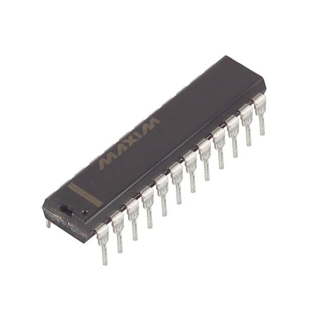
- Part No.:
- DS2176
- Manufacturer:
- Analog Devices Inc./Maxim Integrated
- Category:
- Telecom
- Package:
- 24-DIP (0.300", 7.62mm)
- Datasheet:
-
 DS2176.pdf
- Description:
- IC TELECOM INTERFACE 24DIP
- Quantity:
- Payment:

- Shipping:

Inventory:2,442
Please send an inquiry. Send us your inquiry, and we will respond immediately.
Product details
Overview
DS2176 from Dallas Semiconductor (now Maxim Integrated) is a low-power CMOS T1 receive buffer IC designed to synchronize loop-timed T1 PCM data streams (1.544 MHz) to system-side timing, extract and supervise robbed-bit ABCD signaling, and provide slip-compensated multiframe alignment. It features a 2-frame (386-bit) buffer, 24-pin DIP or 28-pin PLCC package, industrial temperature range (–40°C to +85°C for DS2176N), and compatibility with DS2180A transceivers in digital trunk and cross-connect applications.
For engineers reviewing the DS2176 datasheet, DS2176 pinout, DS2176 application, or DS2176 equivalent, key selection considerations include frame-slip handling at boundary-aligned intervals, robbed-bit signaling extraction under 193S/193E framing, dual-clock support (1.544/2.048 MHz), open-collector SLIP output timing (65 SYSCLK cycles), and signaling freeze behavior during alarm conditions.
Technical Context
The DS2176 implements a dual-clock, dual-domain synchronization architecture: RCLK (1.544 MHz) clocks incoming serial data on its falling edge, while SYSCLK (1.544 or 2.048 MHz) controls system-side output timing on its rising edge. Buffer depth is monitored in real time via RMSYNC–SMSYNC phase relationship, triggering frame slips only at multiframe boundaries when the 2-frame buffer empties or fills completely.
Signaling supervision uses configurable integration (SM0/SM1-selectable 1–5 multiframes) and freeze logic: SIGFRZ asserts high during internal slip or external SIGH assertion, holding A/B/C/D outputs at prior state until SMSYNC rising edge. Signaling updates occur once per multiframe, synchronized to SMSYNC, with SBIT8 enabling reinsertion of extracted bits into outgoing streams.
Key Specifications
| Parameter | Value and Actual Design Meaning |
|---|---|
| Buffer Depth | 2-frame (386-bit); enables short-term jitter absorption without bit errors, slips only at frame boundaries. |
| Input Clock Range | RCLK = 1.544 MHz ± 50 ppm; supports standard T1 line timing with precise falling-edge sampling. |
| System Clock Options | SYSCLK = 1.544 MHz (SCLKSEL = 0) or 2.048 MHz (SCLKSEL = 1); selects framing mode and F-bit handling. |
| Signaling Outputs | A/B/C/D - TTL-compatible, updated once per multiframe at SMSYNC rising edge; C/D mirror A/B in 193S mode. |
| Slip Indication | SLIP - active-low open-collector output held low for exactly 65 SYSCLK cycles per slip event. |
| Supply Voltage | VDD = 4.5 V to 5.5 V; operates at 5 V nominal with IDD = 5–10 mA typical (0°C to 70°C). |
| Temperature Range | Industrial grade: –40°C to +85°C for DS2176N variant; commercial grade: 0°C to 70°C for base DS2176. |
Pinout & Package
DS2176 is available in 24-pin 300-mil DIP (dual in-line package) and 28-pin PLCC (plastic leaded chip carrier) variants. The DS2176N designation refers to the industrial-temperature version in either package.
| Pin/Terminal | Circuit Role | Design Meaning |
|---|---|---|
| RCLK | Input clock | Primary 1.544 MHz receive clock; samples RSER on falling edge. |
| RSER | Input data | Serial T1 data input, synchronized to RCLK falling edge. |
| SYSCLK | Input clock | System-side 1.544/2.048 MHz clock; controls SSER, A/B/C/D, SMSYNC timing. |
| SSER | Output data | System-synchronized serial output; updated on rising edge of SYSCLK. |
| A, B, C, D | Output signals | Robbed-bit signaling bits; valid per channel time, repeated across all frames in multiframe. |
| SLIP | Output indicator | Active-low open-collector signal held low for 65 SYSCLK cycles during frame slip. |
| SMSYNC | Output sync | Slip-compensated system multiframe sync pulse; rising edge marks signaling update point. |
| SIGFRZ | Output flag | High during signaling freeze (slip or SIGH asserted); indicates stale A/B/C/D data. |
| ALN | Input control | Low pulse recenters buffer at next SFSYNC rising edge; may induce slip if depth non-optimal. |
| SIGH | Input control | External signaling inhibit; forces SIGFRZ high and freezes A/B/C/D updates until released. |
Key Features
| Feature | Design Value |
|---|---|
| Frame-boundary slip handling | Ensures no bit loss or corruption during frequency mismatch; slips occur only at multiframe edges, preserving data integrity. |
| Configurable signaling integration | SM0/SM1 select 1–5 multiframe integration depth to suppress noise-induced signaling errors without excessive latency. |
| Slip-compensated signaling sync | SMSYNC output aligns signaling updates to system timing even after slips, enabling deterministic reinsertion via SBIT8. |
| Dual-framing support | FMS pin selects 193S (D4) or 193E (extended) framing, adapting to North American or ETSI T1/E1 infrastructure. |
| Parallel/serial backplane compatibility | S/P pin configures look-ahead (parallel) or direct (serial) output timing, reducing external logic in PABX and DACS designs. |
Applications
| Digital Trunk Interfaces | T1 Drop-and-Insert Equipment |
|---|---|
Use Scenario: Interfacing T1 lines from central office to PBX or media gateway with mismatched timing domains. IC Role / Device Role / Timing Role: Receive-side T1 buffer and signaling supervisor; synchronizes loop-timed data to system clock and extracts ABCD bits. Use Value: Eliminates discrete flip-flop banks and glue logic by integrating 2-frame buffering, slip detection, and signaling freeze in one 24-pin IC. |
Use Scenario: Extracting or inserting individual T1 channels in network monitoring or test systems. IC Role / Device Role / Timing Role: Timing bridge between line-side and system-side clocks; provides SBIT8 and SMSYNC for precise robbed-bit reinsertion timing. Use Value: Enables clean channel passthrough while allowing selective signaling reinsertion without corrupting payload data. |
| Digital Cross-Connect Systems (DACS) | PABX-to-Computer Interfaces (DMI/CPI) |
Use Scenario: Dynamic T1 path switching in carrier-grade cross-connects requiring stable multiframe alignment. IC Role / Device Role / Timing Role: Multiframe synchronization engine; RMSYNC–SMSYNC phase monitoring enables real-time buffer depth visibility. Use Value: Supports hitless reconfiguration by detecting impending slips and maintaining signaling continuity during topology changes. |
Use Scenario: Connecting legacy PABX systems to CTI servers or call recording platforms over T1. IC Role / Device Role / Timing Role: Signaling translator and timing adapter; converts robbed-bit signaling to parallel A/B/C/D outputs synchronized to host CPU clock. Use Value: Provides deterministic, freeze-protected signaling data for call control applications where alarm-induced signaling glitches must be avoided. |
Equivalent & Alternatives
The following parts are listed as comparable options for similar T1 receive buffer and signaling supervision applications.
| Alternative Part | Technical Difference | Application Difference | Selection Advice |
|---|---|---|---|
| DS2180A | Integrated T1 transceiver (line driver + receiver + buffer); includes DS2176 functionality plus transmit path and line interface. | Replaces DS2176 only when full transceiver capability is needed; not a drop-in replacement due to different pinout and added transmit functions. | Select DS2180A when designing new T1 line cards requiring both transmit and receive paths; retain DS2176 for receive-only upgrades or space-constrained receive-buffer-only slots. |
| MC145508 | Single-chip T1/E1 framer + buffer; supports both T1 and E1, but lacks dedicated signaling integration and freeze logic; requires external logic for robust signaling handling. | Used in mixed T1/E1 environments; less suitable for pure T1 signaling-critical applications like PABX interfaces where DS2176's ABCD freeze and integration are essential. | Choose MC145508 for multi-standard (T1/E1) framer applications; prefer DS2176 where deterministic robbed-bit supervision, low-latency slip response, and industrial temp operation are primary requirements. |
Compared with DS2180A and MC145508, the DS2176 delivers optimized, standalone T1 receive buffering with superior signaling supervision granularity (per-multiframe freeze, configurable integration), minimal footprint (24-pin DIP), and guaranteed industrial temperature operation in DS2176N form-making it ideal for embedded telecom infrastructure where reliability and signaling fidelity outweigh multi-standard flexibility.
Availability
DS2176 is available at Aetrix Electronics and suitable for digital trunk interfaces, T1 drop-and-insert equipment, and digital cross-connect systems requiring stable component supply, long-lifecycle availability, and industrial-temperature performance.
Supply support for DS2176 includes scheduled delivery planning, volume procurement assistance, BOM continuity management, traceable sourcing, and lifecycle availability coordination for OEM customers, industrial embedded developers, connected-device designers, and electronics production programs.
Manufacturer
Dallas Semiconductor, now part of Maxim Integrated (acquired 2001), specialized in precision timing, data communications, and mixed-signal interface ICs for telecom and industrial applications.
The DS2176 belongs to Dallas' T1/E1 interface product line, engineered specifically for robust receive-side synchronization and robbed-bit signaling supervision in carrier-class digital telephony equipment.
FAQ
What is the primary function of the DS2176 in a T1 system?
The DS2176 serves as a receive-side T1 buffer and signaling supervisor. Its core functions are synchronizing loop-timed T1 PCM data (1.544 MHz) to system-side timing using a 2-frame buffer, and extracting, freezing, and integrating robbed-bit ABCD signaling embedded in the data stream. In the DS2176, these operations occur independently of transmit functions, making it ideal for receive-only applications such as digital trunk termination and PABX interfaces where signaling integrity is critical.
How does the DS2176 handle frame slips, and what is the role of the SLIP pin?
The DS2176 detects buffer underflow or overflow and triggers a frame slip only at multiframe boundaries to preserve data integrity. When a slip occurs, the SLIP pin-a dedicated active-low open-collector output-is pulled low for exactly 65 SYSCLK cycles. This precise timing allows external logic to detect and respond to slips deterministically. In the DS2176, SLIP assertion coincides with automatic buffer recentering and signaling freeze via SIGFRZ, ensuring no corrupted signaling updates during resynchronization.
What framing standards does the DS2176 support, and how is framing selected?
The DS2176 supports both 193S (D4) and 193E (extended) T1 framing formats. Framing selection is controlled by the FMS (Frame Mode Select) pin: tying FMS low selects 193S framing (A/B signaling in frames 6 and 12), while tying FMS high selects 193E framing (A/B/C/D signaling in frames 6, 12, 18, and 24). This hardware-selectable configuration ensures compatibility with North American (193S) and international (193E) T1 infrastructure without firmware changes. The DS2176 maintains correct signaling mapping and timing for both modes.
Can the DS2176 operate with both 1.544 MHz and 2.048 MHz system clocks, and how is clock selection managed?
Yes, the DS2176 supports both 1.544 MHz (T1) and 2.048 MHz (E1) system clock rates. Clock selection is controlled by the SCLKSEL pin: tying SCLKSEL low configures the device for 1.544 MHz operation (passing the F-bit through SSER), while tying it high configures 2.048 MHz operation (dropping the F-bit and shifting MSB timing). The DS2176 adjusts its internal slip-detection logic and output timing accordingly-ensuring correct buffering, signaling alignment, and SBIT8 positioning for each clock domain without external reconfiguration.
What is the purpose of the SIGFRZ and SIGH pins in the DS2176, and how do they interact?
SIGFRZ is an output that goes high whenever signaling updates to A/B/C/D are frozen-either due to an internal slip condition or external assertion of the SIGH input. SIGH is an input that, when driven low, forces immediate signaling freeze regardless of buffer state. In the DS2176, this interaction provides deterministic control over signaling stability: during alarms or maintenance events, asserting SIGH guarantees stale but consistent signaling data is held, while SIGFRZ provides feedback to system logic that updates are suspended. Both functions are fully supported across all framing and clock modes.
DS2176 Specifications
- Product attributes
- Attribute value
- Manufacturer:
- Analog Devices Inc./Maxim Integrated
- Series:
- -
- Package/Case:
- 24-DIP (0.300", 7.62mm)
- Packaging:
- Tube
- Product Status:
- Obsolete
- Function:
- Receive Buffer
- Interface:
- TDM
- Number of Circuits:
- 1
- Voltage - Supply:
- -
- Current - Supply:
- 5mA
- Power (Watts):
- -
- Operating Temperature:
- 0°C ~ 70°C
- Grade:
- -
- Qualification:
- -
- Mounting Type:
- Through Hole
- Supplier Device Package:
- 24-PDIP
DS2176 FAQ
1.How can I place an order for DS2176 through Aetrix?
Please submit a Request for Quotation (RFQ) for DS2176 on Aetrix. Our sales agent will provide a competitive quotation and guide you through the order confirmation once you accept the terms.
2.Are the price and stock information for DS2176 reliable?
The price and inventory of DS2176 are updated periodically and may fluctuate due to market conditions. Stock and pricing data are typically refreshed every 24 hours. Quotation validity for DS2176 is usually 5 days.
3.What payment methods are accepted for DS2176?
We accept Wire Transfer, PayPal, Credit Card, Western Union, MoneyGram, and Escrow for DS2176 transactions.
Note: Certain payment methods may incur a processing fee.
4.How is shipping managed for DS2176?
DS2176 orders can be shipped via leading logistics carriers, including DHL, UPS, FedEx, TNT, or Registered Mail.
Once your DS2176 order is processed, you will receive an email with the shipment details and tracking number.
Note: Tracking information may take up to 24 hours to appear. Express delivery typically takes 3–5 business days.
5.How can I obtain technical support or documentation for DS2176?
For technical support, including DS2176 datasheets, pinout diagrams, or application guidance, please contact our engineering support team. They can provide detailed documentation and assistance for your DS2176 requirements.
6.How does Aetrix verify that DS2176 is sourced from the original manufacturer or authorized distributors?
All DS2176 products on Aetrix are procured from qualified distributors and authorized channels. Our dedicated quality assurance team conducts strict verification, including traceability checks and, if necessary, third-party testing. This ensures that DS2176 meets industry standards.
7.What is the process for return or replacement of DS2176?
All DS2176 units undergo pre-shipment inspection (PSI). If there is an issue with DS2176, returns or replacements are accepted under the following conditions:
1.Quantity discrepancies, incorrect items, or visible external defects (such as breakage or corrosion), acknowledged by Aetrix.
2.The issue is reported within 90 days of delivery.
3.The DS2176 part is unused and in its original packaging.
Return procedure for DS2176:
1.Submit a request within 90 days.
2.Obtain a Return Material Authorization (RMA) from Aetrix.
DS2176 Tags

-
LMC567CMX/NOPB
Texas Instruments
-
LM567CMX/NOPB
Texas Instruments
-
LM567CM/NOPB
Texas Instruments

-
VSC8531XMW-02
Microchip Technology
-
VSC8531XMW-05
Microchip Technology

-
GPY115C0VI
MaxLinear, Inc.

-
SI32185-A-FMR
Skyworks Solutions Inc.

-
VSC8541XMV-05
Microchip Technology

-
SI32178-B-FM1R
Skyworks Solutions Inc.
-
GPY215C0VI
MaxLinear, Inc.

-
CPC7514ZTR
Littelfuse Inc.

-
VSC8502XML-03
Microchip Technology
Tech Hub

A practical engineering guide to 3.3V and 5V logic compatibility, input thresholds, resistor dividers, translator ICs, MOSFET level shifting, I2C pull-ups, timing limits and power-sequencing risks.

The 74HC595 uses push-pull logic outputs, while the TPIC6B595 uses 50 V open-drain DMOS sinks for higher-power loads. This guide compares timing, current limits, 3.3 V interfacing, load wiring, thermal…

The 74HC595 converts serial data into eight stable parallel outputs. This guide covers pin functions, shift and storage timing, OE and MR behavior, drive-current limits, cascading, voltage compatibilit…

A technical comparison of level-sensitive latches and edge-triggered flip-flops, covering timing windows, setup and hold limits, master–slave operation, time borrowing, race-through, HDL inference and…

A D latch stores one bit while Enable controls when data can pass. This reference covers gate-level operation, truth tables, transparency, setup and hold timing, LE versus OE, common ICs and practical …

An SR latch stores one bit through cross-coupled feedback. This engineering reference covers NOR and NAND implementations, truth tables, forbidden-state recovery, gated operation, switch debouncing, fa…

Latch circuits retain one bit through feedback. This technical reference covers SR and D latches, truth tables, transparency, timing limits, latch-versus-flip-flop behavior, applications and common log…

An engineering guide to LED driver operation, constant-current and constant-voltage outputs, linear and switching topologies, dimming, IC selection, calculations, replacement compatibility, and fault c…

Operational amplifier guide covering op amp basics, feedback, ideal vs real op amps, common configurations, buffer circuits, offset, bias current, gain-bandwidth, slew rate, rail-to-rail limits and sel…

Jumper cables guide covering safe connection order, red and black clamp placement, final ground connection, cable gauge, length, clamp quality, copper vs CCA cables, jump starter comparison and battery…


