
 My Inquiry
 My Account


Analog Devices Inc./Maxim Integrated DS2176QN
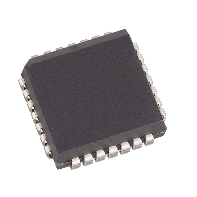
- Part No.:
- DS2176QN
- Manufacturer:
- Analog Devices Inc./Maxim Integrated
- Category:
- Telecom
- Package:
- 28-LCC (J-Lead)
- Datasheet:
-
 DS2176QN.pdf
- Description:
- IC TELECOM INTERFACE 28PLCC
- Quantity:
- Payment:

- Shipping:

Inventory:1,027
Please send an inquiry. Send us your inquiry, and we will respond immediately.
Product details
Overview
DS2176QN from Maxim Integrated (now Analog Devices) is a low-power CMOS T1 receive buffer IC designed to synchronize loop-timed T1 PCM data streams (1.544 MHz) to system-side timing while extracting and supervising robbed-bit ABCD signaling. It features a 2-frame (386-bit) FIFO buffer, slip detection on frame boundaries, open-collector SLIP output active low for 65 SYSCLK cycles, and supports both 193S and 193E framing modes via FMS pin. Used in digital cross-connects and PABX-to-computer interfaces.
For engineers reviewing the DS2176QN datasheet, DS2176QN pinout, DS2176QN application, or DS2176QN equivalent, key selection criteria include its dual-clock compatibility (1.544/2.048 MHz), signaling freeze control via SIGFRZ, external buffer recentering via ALN, and explicit support for serial/parallel backplane interfacing with S/P select.
Technical Context
The DS2176QN implements a 2-frame deep FIFO with real-time buffer depth monitoring via RMSYNC–SMSYNC edge spacing. Slip correction occurs only at frame boundaries, and the device enforces signaling update inhibition during alarm or slip conditions using internal freeze logic tied to SM0/SM1 configuration.
It extracts ABCD bits from T1 frames-A/B in 193S (FMS=0), A/B/C/D in 193E (FMS=1)-and integrates them across 1–5 multiframes depending on SM0/SM1 settings. Signaling updates are slip-compensated and synchronized to SMSYNC rising edges, with SBIT8 providing LSB timing for reinsertion into outgoing streams.
Key Specifications
| Parameter | Value and Actual Design Meaning |
|---|---|
| Supply Voltage | 4.5 V to 5.5 V - ensures stable operation under standard 5 V TTL-compatible systems with ±10% tolerance. |
| Operating Temperature | –40°C to +85°C - industrial-grade thermal range enabling deployment in telecom central office and remote terminal environments. |
| Receive Clock (RCLK) | 1.544 MHz - precisely matches T1 line rate; sampled on falling edge for RSER input capture. |
| System Clock (SYSCLK) | 1.544 MHz or 2.048 MHz - selectable via SCLKSEL; determines buffer read rate and F-bit handling (passed vs. dropped). |
| Buffer Depth | 2-frame (386 bits) - provides jitter tolerance without excessive latency; slips occur only at frame boundaries to preserve data integrity. |
| Signaling Outputs | A, B, C, D - valid per channel time; updated once per multiframe at SMSYNC rising edge unless frozen by slip or SIGH. |
| SLIP Output | Active-low open-collector, held low for 65 SYSCLK cycles - enables external slip event detection and system-level synchronization response. |
Pinout & Package
DS2176QN is packaged in a 24-pin 300-mil DIP (dual in-line package) with through-hole mounting, rated for industrial temperature operation (–40°C to +85°C). Pin numbering follows standard DIP layout with Pin 1 at top-left corner.
| Pin/Terminal | Circuit Role | Design Meaning |
|---|---|---|
| 1 (SIGN) | Input | Disables ABCD signaling updates when low; duration controlled by SM0/SM1 or until returned high. |
| 2 (RMSYNC) | Input | Establishes receive-side frame/multiframe alignment on rising edge; used with SMSYNC to monitor buffer depth. |
| 3 (RCLK) | Input | 1.544 MHz receive clock; RSER data sampled on falling edge for precise T1 bit alignment. |
| 4 (RSER) | Input | Serial T1 data input; synchronous to RCLK falling edge, feeding the 2-frame FIFO buffer. |
| 5–8 (A, B, C, D) | Output | Robbed-bit signaling outputs; A/B valid in 193S, all four valid in 193E framing; updated once per multiframe. |
| 9 (SCHCLK) | Output | System channel clock; transitions high at channel boundaries to aid serial-to-parallel conversion. |
| 10–11 (SM0, SM1) | Input | Select signaling supervision mode: integration depth (1–5 multiframes), freeze duration, and framing behavior. |
| 12 (VSS) | Power | Signal ground reference (0 V); decoupling required near VDD/VSS pins for noise immunity. |
| 13 (S/P) | Input | Selects interface mode: tied to VSS for parallel backplanes, VDD for serial backplanes. |
| 14 (FMS) | Input | Framing mode select: 0 = 193S (A/B only), 1 = 193E (A/B/C/D); defines signaling bit positions in multiframe. |
| 15 (ALN) | Input | Forces buffer recentering on next system frame boundary; may induce a slip if depth adjustment is needed. |
| 16 (SFSYNC) | Input | Rising edge establishes system-side frame start; synchronizes SSER output and SMSYNC generation. |
| 17 (SIGFRZ) | Output | High during signaling freeze (slip/alarm/SIGH low); indicates when ABCD outputs hold previous values. |
| 18 (SMSYNC) | Output | Slip-compensated multiframe sync; rising edge marks signaling update point; pulse width = 65 SYSCLK cycles. |
| 19 (SBIT8) | Output | Indicates LSB position of each channel; enables external logic to reinsert signaling bits into outgoing SSER stream. |
| 20 (SLIP) | Output | Open-collector active-low slip indicator; asserted for exactly 65 SYSCLK cycles upon buffer under/overflow. |
| 21 (SSER) | Output | System serial output; updated on rising edge of SYSCLK; carries synchronized PCM data with optional F-bit handling. |
| 22 (SYSCLK) | Input | System clock (1.544 or 2.048 MHz); controls SSER, SMSYNC, SIGFRZ timing and buffer read rate. |
| 23 (SCLKSEL) | Input | Selects SYSCLK frequency: 0 = 1.544 MHz (F-bit passed), 1 = 2.048 MHz (F-bit dropped, MSB shifted). |
| 24 (VDD) | Power | +5 V supply; must be decoupled with 0.1 µF ceramic capacitor close to pin for stable CMOS operation. |
Key Features
| Feature | Design Value |
|---|---|
| Two-frame FIFO buffer | Enables deterministic slip occurrence only at frame boundaries, preserving data coherency during frequency mismatch. |
| Slip-compensated signaling output (SMSYNC) | Delivers timing-stable signaling updates aligned to system multiframe, eliminating phase drift in downstream processing. |
| Configurable signaling integration (SM0/SM1) | Reduces false signaling updates caused by line noise by requiring consistent bit state across 1–5 multiframes before output change. |
| External buffer recentering (ALN) | Allows deterministic initialization or recovery after power-up/reset without relying on automatic slip-based recentering. |
| Parallel/serial backplane compatibility (S/P) | Supports both architectures with identical IC: S/P=0 enables look-ahead parallel timing; S/P=1 configures serial output mode. |
Applications
| Digital Cross-Connect Systems (DACS) | PABX-to-Computer Interface (DMI/CPI) |
|---|---|
Use Scenario: Interfacing T1 trunks between legacy circuit-switched networks and packet-based control systems. IC Role / Device Role / Timing Role: Receives loop-timed T1 data, synchronizes it to system clock, and extracts ABCD signaling for call setup/teardown. Use Value: Eliminates discrete glue logic for frame alignment and signaling extraction, reducing board space and improving timing predictability. |
Use Scenario: Bridging private branch exchange (PABX) signaling with host computer applications like CTI or voicemail. IC Role / Device Role / Timing Role: Acts as T1 receive buffer and signaling supervisor, delivering clean, slip-compensated ABCD bits to host processor via parallel backplane. Use Value: Enables reliable DMI/CPI protocol compliance by freezing signaling during slips and aligning updates to SMSYNC for deterministic software polling. |
| Digital Trunk Interfaces | Drop-and-Insert Equipment |
Use Scenario: Aggregating multiple T1 lines into higher-speed backplanes in central office switching systems. IC Role / Device Role / Timing Role: Converts loop-timed T1 streams to system-synchronized data while maintaining robbed-bit signaling integrity across frame boundaries. Use Value: Provides consistent 2-frame latency and open-collector SLIP output for centralized slip management across multi-channel systems. |
Use Scenario: Inserting/removing individual channels from T1 data streams without disrupting adjacent channels or signaling. IC Role / Device Role / Timing Role: Buffers incoming T1 data and supplies SBIT8 timing signal to enable precise bit-level reinsertion of extracted signaling bits. Use Value: Allows off-chip logic to reconstruct full T1 frames with updated signaling, supporting dynamic channel provisioning and maintenance functions. |
Equivalent & Alternatives
The following parts are listed as comparable options for similar T1 receive buffer and signaling supervision applications.
| Alternative Part | Technical Difference | Application Difference | Selection Advice |
|---|---|---|---|
| DS2176Q | Commercial temperature range (0°C to +70°C); same pinout and functionality as DS2176QN but lacks industrial-grade thermal rating. | Restricted to controlled-environment applications such as lab equipment or non-central-office telecom gear. | Select DS2176Q only when ambient operating temperature remains within 0–70°C and industrial reliability is not required. |
| DS2180A | Integrated T1 transceiver (line driver + receiver + buffer); includes DS2176QN's receive buffer functionality plus transmit path and line interface. | Replaces separate transceiver + buffer designs; requires different PCB layout and external line transformer. | Choose DS2180A when full T1 transceiver capability is needed; DS2176QN remains optimal for receive-only buffering with existing line drivers. |
Compared with DS2176Q, DS2176QN offers extended thermal operation critical for outdoor cabinets and uncooled enclosures; compared with DS2180A, DS2176QN provides lower power, smaller footprint, and design flexibility when transmit functionality is handled separately.
Availability
DS2176QN is available at Aetrix Electronics and suitable for digital cross-connect systems, PABX-to-computer interfaces, and T1 trunk aggregation requiring stable component supply, long-term lifecycle support, and industrial temperature performance.
Supply support for DS2176QN includes scheduled delivery planning, volume procurement assistance, BOM continuity management, traceable sourcing, and lifecycle availability coordination for OEM customers, industrial embedded developers, connected-device designers, and electronics production programs.
Manufacturer
Analog Devices (formerly Maxim Integrated) is a global semiconductor leader specializing in high-performance analog, mixed-signal, and digital signal processing technologies for communications, industrial, and automotive markets.
The DS2176QN belongs to Maxim's legacy T-carrier interface product line, engineered specifically for telecom infrastructure applications requiring precise T1 receive synchronization, robbed-bit signaling supervision, and industrial-grade reliability.
FAQ
What is the primary function of the DS2176QN in a T1 system?
The DS2176QN serves as a receive-side T1 buffer that synchronizes loop-timed 1.544 MHz PCM data to system clock domains while extracting and supervising robbed-bit ABCD signaling. Its 2-frame FIFO ensures slips occur only at frame boundaries, and it delivers slip-compensated signaling updates via SMSYNC-making DS2176QN essential for deterministic timing in digital cross-connects and PABX interfaces.
How does the DS2176QN handle different T1 framing standards?
The DS2176QN supports both 193S and 193E framing via the FMS pin: FMS=0 selects 193S (A/B signaling only), FMS=1 selects 193E (A/B/C/D signaling). Signaling bit positions are fixed per standard-A in frame 6, B in frame 12 for 193S; C in frame 18, D in frame 24 for 193E-and DS2176QN outputs valid A/B/C/D signals accordingly, with C/D holding prior multiframe data in 193S mode.
What is the role of the SLIP output on the DS2176QN?
The SLIP output on DS2176QN is an active-low, open-collector signal asserted for exactly 65 SYSCLK cycles whenever the 2-frame buffer underflows or overflows. It provides a hardware-level slip event indicator for system-level fault handling, enabling external logic to pause processing, log events, or trigger recovery-without requiring software polling of internal status registers, since DS2176QN has no serial interface or status register.
Can the DS2176QN operate with a 2.048 MHz system clock?
Yes, the DS2176QN supports 2.048 MHz system clock operation when SCLKSEL is tied high. In this mode, the F-bit is dropped from the output stream, and the MSB of channel 1 appears at SSER one bit period after SFSYNC rising edge. Buffer slip criteria are adjusted internally to accommodate faster read rates, ensuring robust synchronization-confirming DS2176QN's dual-rate capability for E1/T1 hybrid systems.
How does the DS2176QN manage signaling updates during alarm conditions?
The DS2176QN freezes ABCD signaling updates during alarm or slip conditions using internal logic that holds previous values at outputs A/B/C/D and asserts SIGFRZ high. This freeze duration is configurable via SM0/SM1 (1–5 multiframes), and forcing SIGH low externally also triggers freeze. DS2176QN ensures signaling integrity by preventing corruption from transient line faults-critical for DS2176QN deployments in mission-critical telecom infrastructure where false signaling could disrupt call control.
DS2176QN Specifications
- Product attributes
- Attribute value
- Manufacturer:
- Analog Devices Inc./Maxim Integrated
- Series:
- -
- Package/Case:
- 28-LCC (J-Lead)
- Packaging:
- Tube
- Product Status:
- Obsolete
- Function:
- Receive Buffer
- Interface:
- TDM
- Number of Circuits:
- 1
- Voltage - Supply:
- -
- Current - Supply:
- 5mA
- Power (Watts):
- -
- Operating Temperature:
- 0°C ~ 70°C
- Grade:
- -
- Qualification:
- -
- Mounting Type:
- Surface Mount
- Supplier Device Package:
- 28-PLCC (11.51x11.51)
DS2176QN FAQ
1.How can I place an order for DS2176QN through Aetrix?
Please submit a Request for Quotation (RFQ) for DS2176QN on Aetrix. Our sales agent will provide a competitive quotation and guide you through the order confirmation once you accept the terms.
2.Are the price and stock information for DS2176QN reliable?
The price and inventory of DS2176QN are updated periodically and may fluctuate due to market conditions. Stock and pricing data are typically refreshed every 24 hours. Quotation validity for DS2176QN is usually 5 days.
3.What payment methods are accepted for DS2176QN?
We accept Wire Transfer, PayPal, Credit Card, Western Union, MoneyGram, and Escrow for DS2176QN transactions.
Note: Certain payment methods may incur a processing fee.
4.How is shipping managed for DS2176QN?
DS2176QN orders can be shipped via leading logistics carriers, including DHL, UPS, FedEx, TNT, or Registered Mail.
Once your DS2176QN order is processed, you will receive an email with the shipment details and tracking number.
Note: Tracking information may take up to 24 hours to appear. Express delivery typically takes 3–5 business days.
5.How can I obtain technical support or documentation for DS2176QN?
For technical support, including DS2176QN datasheets, pinout diagrams, or application guidance, please contact our engineering support team. They can provide detailed documentation and assistance for your DS2176QN requirements.
6.How does Aetrix verify that DS2176QN is sourced from the original manufacturer or authorized distributors?
All DS2176QN products on Aetrix are procured from qualified distributors and authorized channels. Our dedicated quality assurance team conducts strict verification, including traceability checks and, if necessary, third-party testing. This ensures that DS2176QN meets industry standards.
7.What is the process for return or replacement of DS2176QN?
All DS2176QN units undergo pre-shipment inspection (PSI). If there is an issue with DS2176QN, returns or replacements are accepted under the following conditions:
1.Quantity discrepancies, incorrect items, or visible external defects (such as breakage or corrosion), acknowledged by Aetrix.
2.The issue is reported within 90 days of delivery.
3.The DS2176QN part is unused and in its original packaging.
Return procedure for DS2176QN:
1.Submit a request within 90 days.
2.Obtain a Return Material Authorization (RMA) from Aetrix.
DS2176QN Tags

-
LMC567CMX/NOPB
Texas Instruments
-
LM567CMX/NOPB
Texas Instruments
-
LM567CM/NOPB
Texas Instruments

-
VSC8531XMW-02
Microchip Technology
-
VSC8531XMW-05
Microchip Technology

-
GPY115C0VI
MaxLinear, Inc.

-
SI32185-A-FMR
Skyworks Solutions Inc.

-
VSC8541XMV-05
Microchip Technology

-
SI32178-B-FM1R
Skyworks Solutions Inc.
-
GPY215C0VI
MaxLinear, Inc.

-
CPC7514ZTR
Littelfuse Inc.

-
VSC8502XML-03
Microchip Technology
Tech Hub

A practical engineering guide to 3.3V and 5V logic compatibility, input thresholds, resistor dividers, translator ICs, MOSFET level shifting, I2C pull-ups, timing limits and power-sequencing risks.

The 74HC595 uses push-pull logic outputs, while the TPIC6B595 uses 50 V open-drain DMOS sinks for higher-power loads. This guide compares timing, current limits, 3.3 V interfacing, load wiring, thermal…

The 74HC595 converts serial data into eight stable parallel outputs. This guide covers pin functions, shift and storage timing, OE and MR behavior, drive-current limits, cascading, voltage compatibilit…

A technical comparison of level-sensitive latches and edge-triggered flip-flops, covering timing windows, setup and hold limits, master–slave operation, time borrowing, race-through, HDL inference and…

A D latch stores one bit while Enable controls when data can pass. This reference covers gate-level operation, truth tables, transparency, setup and hold timing, LE versus OE, common ICs and practical …

An SR latch stores one bit through cross-coupled feedback. This engineering reference covers NOR and NAND implementations, truth tables, forbidden-state recovery, gated operation, switch debouncing, fa…

Latch circuits retain one bit through feedback. This technical reference covers SR and D latches, truth tables, transparency, timing limits, latch-versus-flip-flop behavior, applications and common log…

An engineering guide to LED driver operation, constant-current and constant-voltage outputs, linear and switching topologies, dimming, IC selection, calculations, replacement compatibility, and fault c…

Operational amplifier guide covering op amp basics, feedback, ideal vs real op amps, common configurations, buffer circuits, offset, bias current, gain-bandwidth, slew rate, rail-to-rail limits and sel…

Jumper cables guide covering safe connection order, red and black clamp placement, final ground connection, cable gauge, length, clamp quality, copper vs CCA cables, jump starter comparison and battery…


